
System and Method for Reading Memory

a static memory and system technology, applied in the field of static memory operation, can solve the problems of slowing down the reading operation, still disadvantages of the access circuit, and large access circuit size, and achieve the effects of convenient data reading, faster reads, and compact structur

Inactive Publication Date: 2011-01-20
VNS PORTFOLIO LLC
View PDF0 Cites 16 Cited by
  • Summary
  • Abstract
  • Description
  • Claims
  • Application Information

AI Technical Summary

Benefits of technology

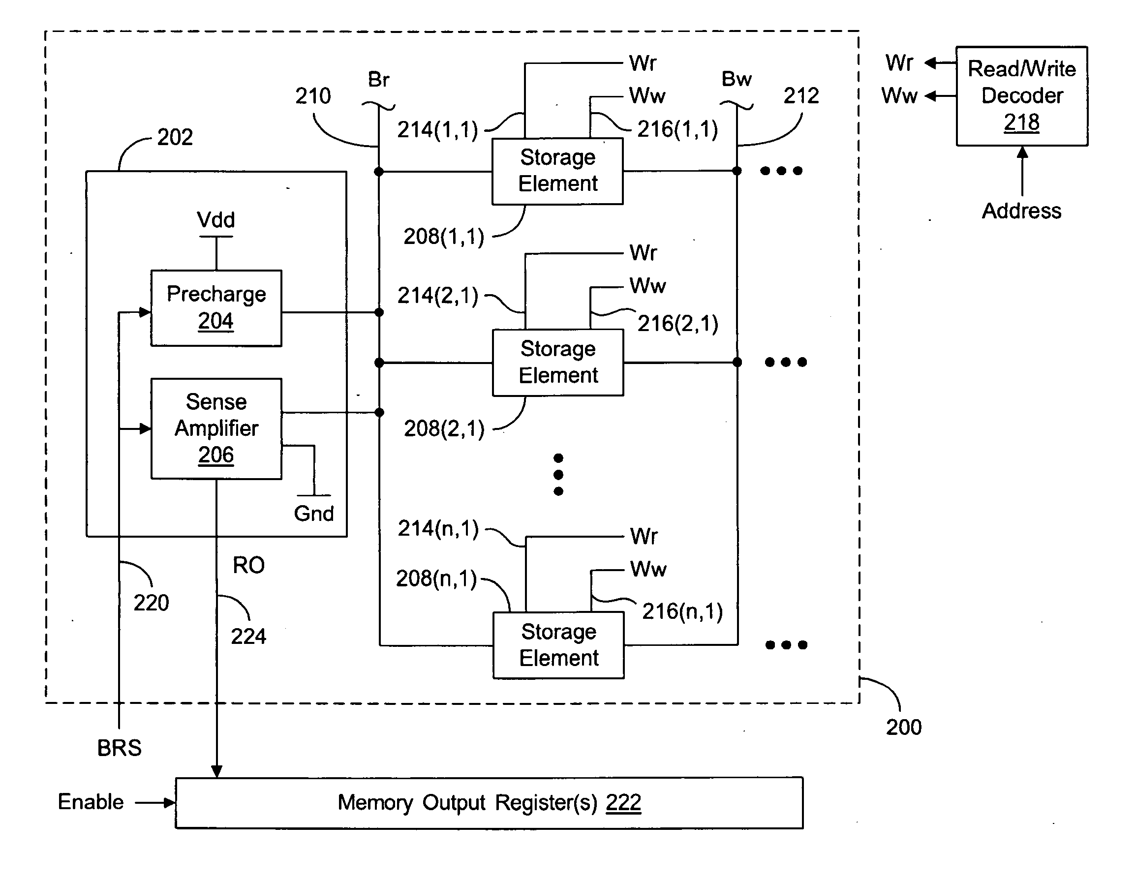
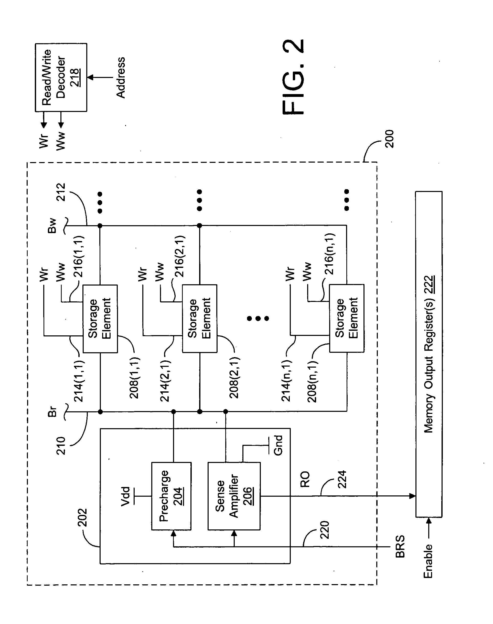
"The present invention provides a memory device that is more compact and faster than previous versions. It achieves this by precharging the bit line and maintaining the precharge while the memory cell is read. This reduces the complexity of the memory access circuitry. The memory includes a bit line for transmitting data bits, a plurality of storage elements that store data bits and are coupled to selectively assert the stored data bits on the bit line, and a precharge circuit that charges the bit line when in a charging state. The precharge circuit remains in the charging state while the storage elements assert data bits on the bit line. The memory also includes a sense amplifier that receives and inverts the data bits and asserts the complement of the data bits on a read output terminal. The memory can be associated with a plurality of processors, which can communicate and operate asynchronously from one another. The method for reading data stored in the memory includes applying a continuous precharge to the bit line, asserting a bit of data from the storage element on the bit line, and maintaining the continuous precharge while the data bit is asserted. The method also includes inverting the data bit and asserting the bit complement on the read output terminal."

Problems solved by technology

However, small cells connected to long wires create a problem for the operating speed, speed being a desirable characteristic of memory, and thus the design of memory access circuits is necessarily a search for optimum solutions for a set of conflicting requirements, which are dependent on the application in each particular case.
However, for small memory with shorter bit lines, access circuit size becomes important because the access circuit size can quickly become too large.
Although prior art precharging circuits provide some advantages, there are still disadvantages to these circuits.
Similarly, turning off the precharge prior to sensing the state of a memory cell also requires extra time in asynchronous circuits, which slows down the reading operation.
Moreover, the control circuitry for turning the precharge off prior to sensing the state of the memory cell can occupy valuable real estate in a crowded integrated circuit.

Method used


Image

  • System and Method for Reading Memory
  • System and Method for Reading Memory
  • System and Method for Reading Memory

Examples


Embodiment Construction

[0023]The present invention overcomes the problems associated with the prior art, by providing a system and method for quickly and efficiently reading data from, for example, Static Random Access Memory (“SRAM”). In the following description, numerous specific details are set forth (e.g., specific circuit layouts) in order to provide a thorough understanding of the invention. Those skilled in the art will recognize, however, that the invention may be practiced apart from these specific details. In other instances, details of well known circuit manufacturing practices (e.g., photolithography, doping, etc.) and components have been omitted, so as not to unnecessarily obscure the present invention.

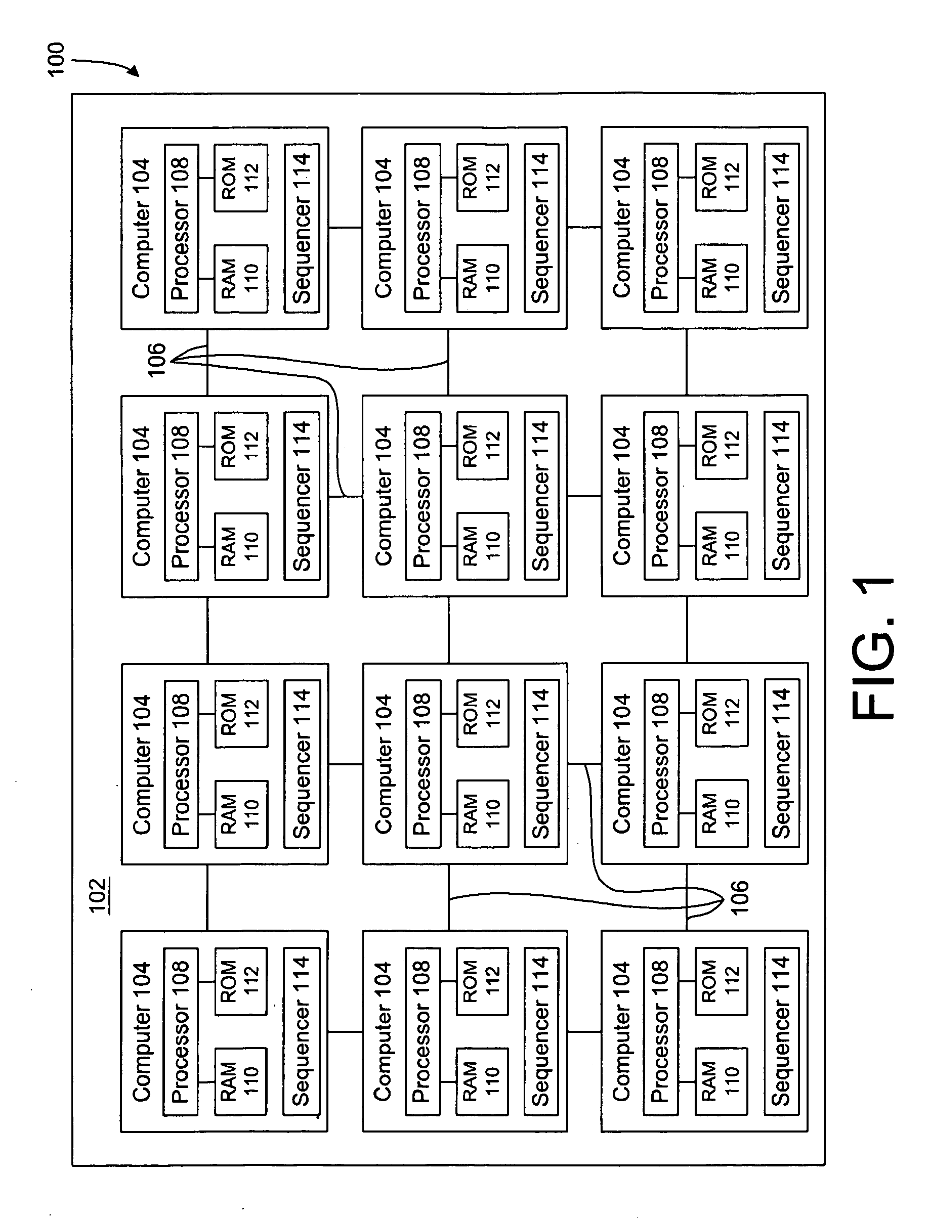
[0024]FIG. 1 shows a computer array 100 formed on a single die 102. Computer array 100 includes a plurality (twelve in this example) of computers 104 (sometimes also referred to as “cores” or “nodes” in the example of an array) interconnected by a plurality of data paths (e.g., buses) 106. Ac...


PUM


Abstract

A novel memory reading circuit includes a bit line for transmitting data bits within the memory, a plurality of storage elements for storing bits of data, and a precharge circuit coupled to the bit line for charging the bit line when the precharge circuit is in a charging state, the precharge circuit being operative to remain in the charging state at time when the storage elements assert the stored bits of data on the bit line. The memory may be a single-ended, static random access memory (“SRAM”). The SRAM circuits of the invention may be incorporated into each of a plurality of individual computers arrayed on a single die.

Description

BACKGROUND OF THE INVENTION[0001]1. Field of the Invention[0002]This invention relates generally to static memory operation, and more particularly to an improved circuit and method for reading a static memory cell, especially for application in single-chip multiprocessor arrays in embedded systems.[0003]2. Description of the Background Art[0004]In the art of computing, speed is a much desired quality, and the quest to create faster computers, processors, and other components is ongoing. In efforts to increase computing speed, various circuits for reading static memory have been designed.[0005]A semiconductor static memory cell typically comprises two cross-coupled MOS inverters connected between a high voltage (Vdd) and a low voltage (Gnd), which have two stable states defined by logical high and logical low potentials at two inverter ports, Q and Q-bar (complement or inverse of Q), respectively. The logical high potential is somewhat lower than Vdd and the logical low potential is ...

Claims


Application Information

Patent Timeline
Patent Type & Authority Applications(United States)
IPC IPC(8): G11C7/00
CPCG11C11/413G11C11/412G11C11/419
Inventor MOORE, CHARLES H.
Owner VNS PORTFOLIO LLC
Learn More