Self-powered lithography method and apparatus using radioactive thin films

a self-powered lithography and thin film technology, applied in photomechanical equipment, instruments, originals for photomechanical treatment, etc., can solve the problems of high production cost and maintenance costs of prior art lithography systems, and achieve the effect of fast and low-cost nano-lithography and low-cost nano-scale systems

Active Publication Date: 2011-01-20
CORNELL UNIVERSITY
View PDF17 Cites 7 Cited by
  • Summary
  • Abstract
  • Description
  • Claims
  • Application Information

AI Technical Summary

Benefits of technology

[0012]The structures and methods of present invention overcome the above mentioned difficulties by providing a practical, working “contact” lithography system, whic

Problems solved by technology

Prior art lithography systems thus require columns o

Method used


Image

  • Self-powered lithography method and apparatus using radioactive thin films
  • Self-powered lithography method and apparatus using radioactive thin films
  • Self-powered lithography method and apparatus using radioactive thin films

Examples


Embodiment Construction

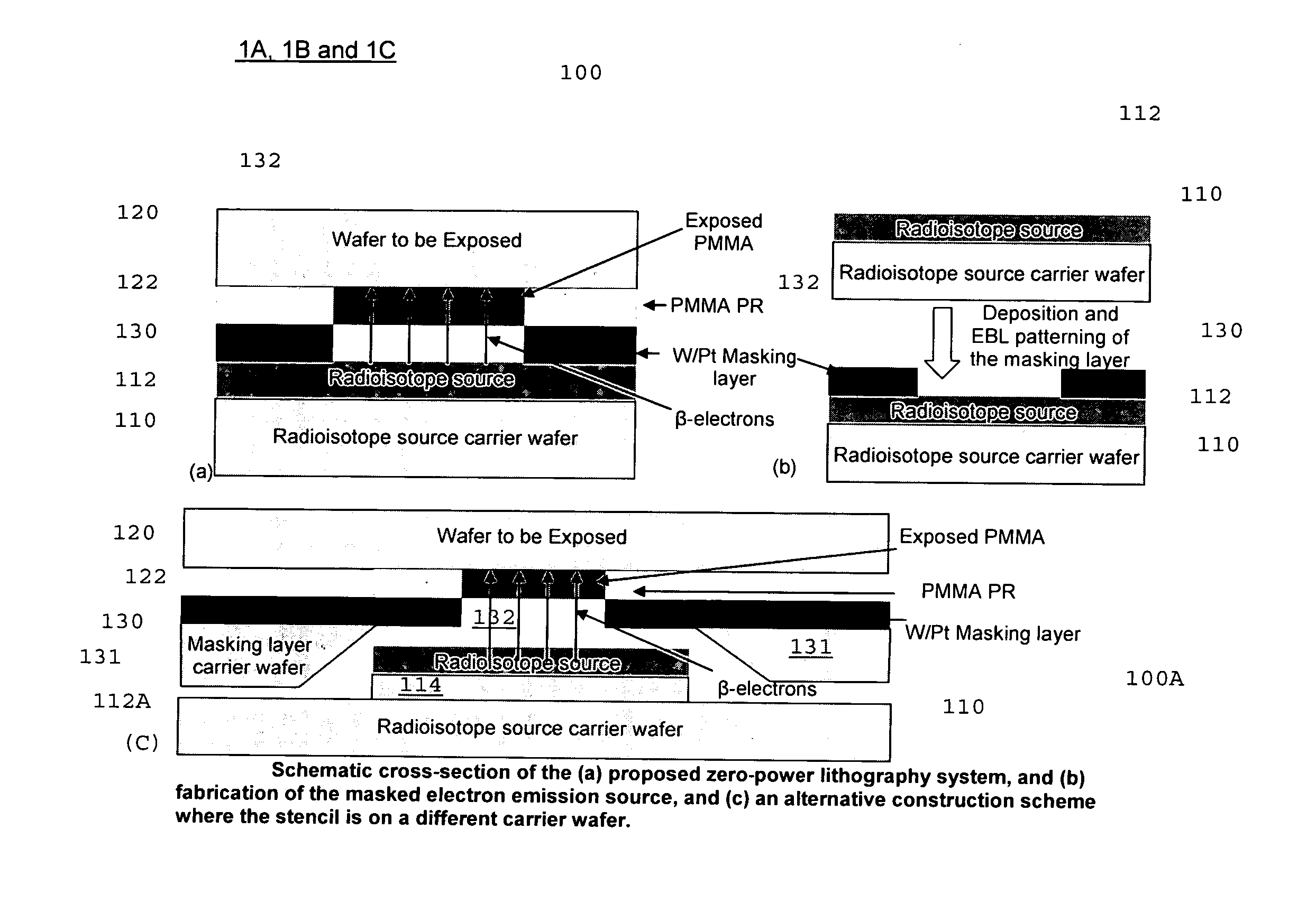
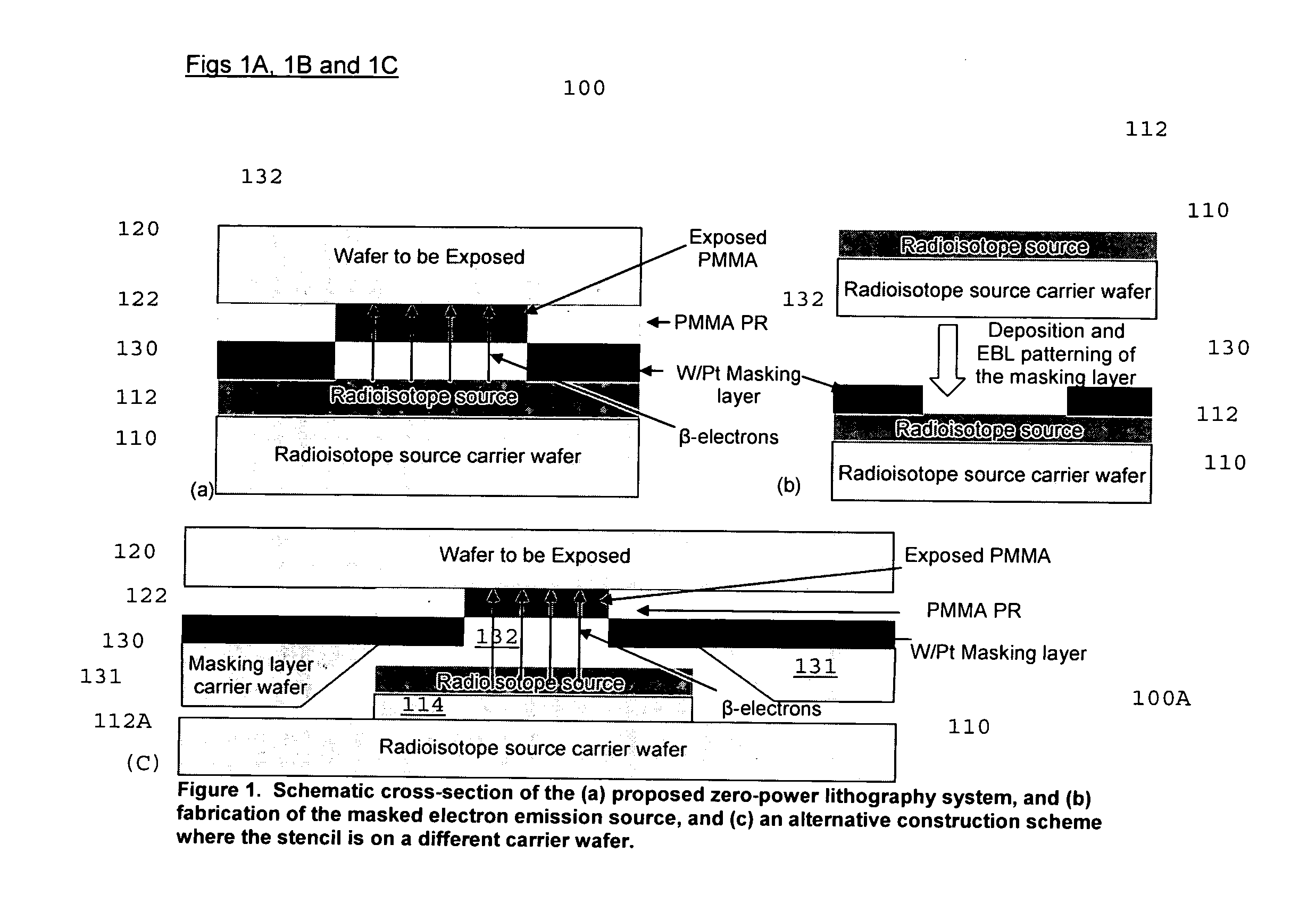
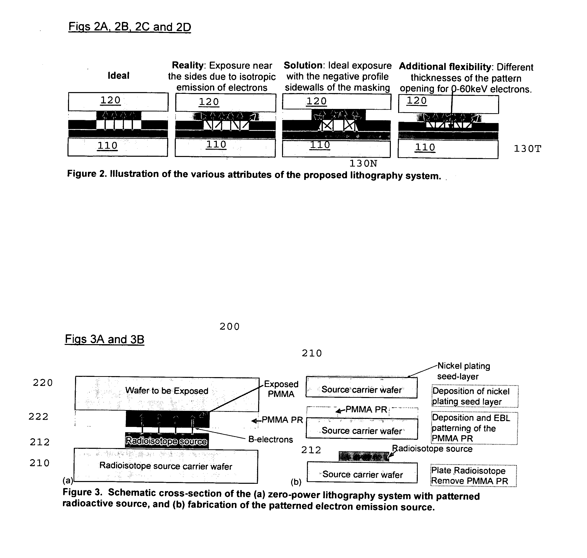
[0042]Turning now to FIGS. 1A-10E, in accordance with the present invention, a lithographic system 100 includes three primary components, namely, an emitter thin film or substrate 110 including the radioactive material 112 (e.g., a radioisotope), a target substrate 120 which carries the energy-modifiable layer 122 (e.g., photo-resist), and a stencil or mask 130 sandwiched or positioned between emitter substrate 110 and target substrate 120. Pattern-defining stencil 130 includes a non-transmissive material (e.g., a heavy metal masking layer made from such as a W / Pt) capable of blocking particles emitted through radioactive decay from radioisotope 112 of the emitter substrate 110.

[0043]Stencil 130 defines a pattern having openings or vias arranged to permit selective transmission of the particles emitted through radioactive decay from the radioisotope of the emitter substrate 110, and stencil 130 is placed up against (or very close to) the target substrate, as shown in FIG. 1A, a sche...


PUM

PropertyMeasurementUnit
Timeaaaaaaaaaa
Lengthaaaaaaaaaa
Lengthaaaaaaaaaa

Abstract

A self-powered ‘near field’ lithographic system 100 includes three primary components, namely, a thin film or emitter substrate 110 including a radioactive material (e.g., a radioisotope 112), a target substrate 120 which carries an energy-modifiable layer 122 (e.g., photo-resist) and a stencil (e.g., 130) that is either positioned between the emitter and target substrates fabricated upon and defined in the emitter substrate. The stencil is made from a material capable of blocking particles emitted through radioactive decay from the radioisotope of the emitter substrate. The stencil includes openings or vias 132 patterned to permit selective transmission of the particles emitted through radioactive decay from the radioisotope of the emitter substrate 110, and the stencil is preferably placed up against (or very close to) the target substrate 120.

Description

PRIORITY CLAIM AND REFERENCE TO RELATED APPLICATION[0001]This application claims priority to related and commonly owned U.S. provisional patent application No. 61 / 008, 596, filed Dec. 21, 2007, the entire disclosure of which is incorporated herein by reference.BACKGROUND OF THE INVENTION[0002]1. Field of the Invention[0003]The present invention relates to methods for fabricating semiconductor circuitry or nano-scale electro-mechanical systems and provides a cost-effective alternative to standard photolithography or electron beam lithography.[0004]2. Discussion of Related Art[0005]Semiconductors and nano-scale electro-mechanical systems have traditionally been produced using processes such as standard photolithography or electron beam lithography, each of which require significant investment in capital equipment and related facilities.[0006]Thin film processing is a cornerstone of modern integrated circuit industry. All integrated circuits consist of successive deposition and removal...

Claims


Application Information

Patent Timeline
IPC IPC(8): H01L21/306G03F7/20
CPCG03F1/14G03F1/20G03F7/2065G03F7/2039G03F1/22
Inventor LAL, AMIT
Owner CORNELL UNIVERSITY
Why Eureka
Try Eureka