Vacuum Coupled Tool Apparatus for Dry Transfer Printing Semiconductor Elements

a technology of transfer printing and tooling, which is applied in the direction of photomechanical equipment, applications, instruments, etc., can solve the problems of inability to economically handle semi-thin semiconductor chips or dies, inability to provide kinetic and shear-assisted control of adhesion, and inability to handle the new class of reinforced composite stamps. achieve the effect of reducing wait time, reducing time required, and improving processing and printing speed

Inactive Publication Date: 2011-01-27
X DISPLAY CO TECH LTD
View PDF65 Cites 26 Cited by
  • Summary
  • Abstract
  • Description
  • Claims
  • Application Information

AI Technical Summary

Benefits of technology

[0041]In an embodiment, the process may be tailored to reduce the time required for the system to achieve pressure equilibrium in the internal cavity after transfer has occurred, such as by providing a negative pressure relative to ambient pressure in the internal cavity after the semiconductor element is transferred. Such reduction in time decreases the wait time required to then print the transferred features, resulting in over-all improved processing and print speed.
[0042]In another aspect, any of the methods and devices further relates to an anti-flexure feature that provides further flexural rigidity to the transfer stamp.

Problems solved by technology

Semiconductor chips or die which are ultra thin, fragile, or too small cannot be economically handled by traditional vacuum grippers.
There are, however, challenges with that technique for use with high fidelity, thin, (e.g., <1 mm) composite stamps.
No. 61/116,136 filed No

Method used


Image

  • Vacuum Coupled Tool Apparatus for Dry Transfer Printing Semiconductor Elements
  • Vacuum Coupled Tool Apparatus for Dry Transfer Printing Semiconductor Elements
  • Vacuum Coupled Tool Apparatus for Dry Transfer Printing Semiconductor Elements

Examples


example 1

Vacuum-Coupled Tool Apparatus

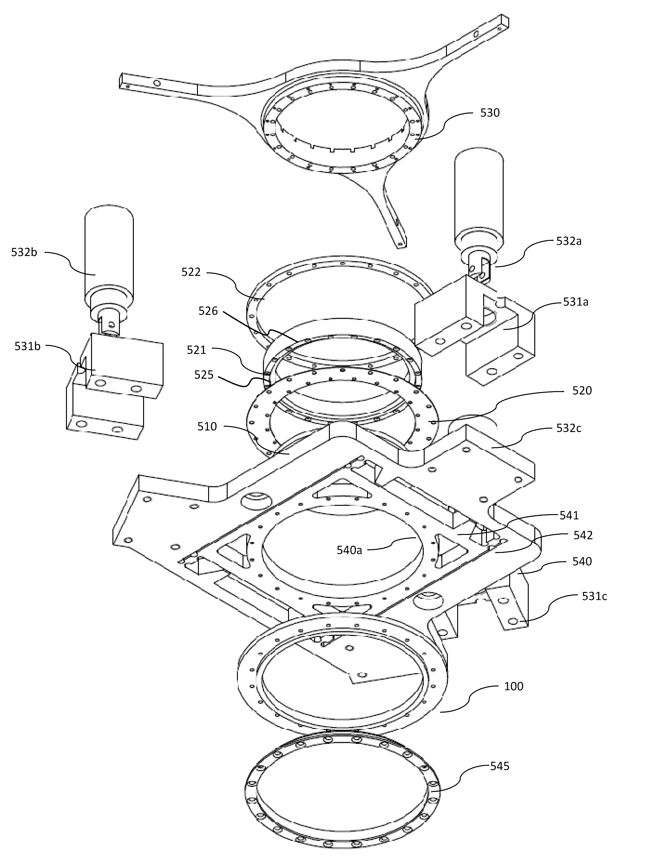
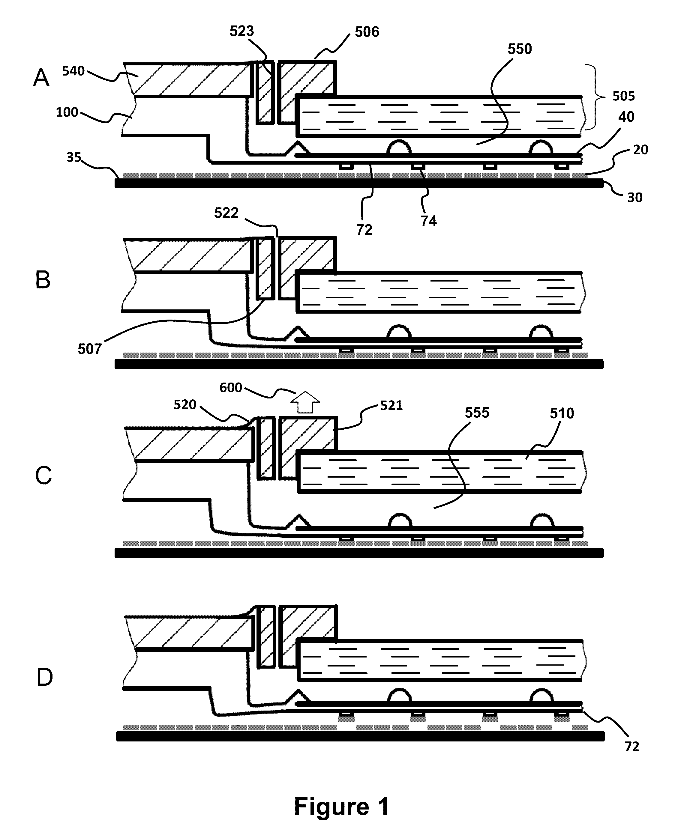
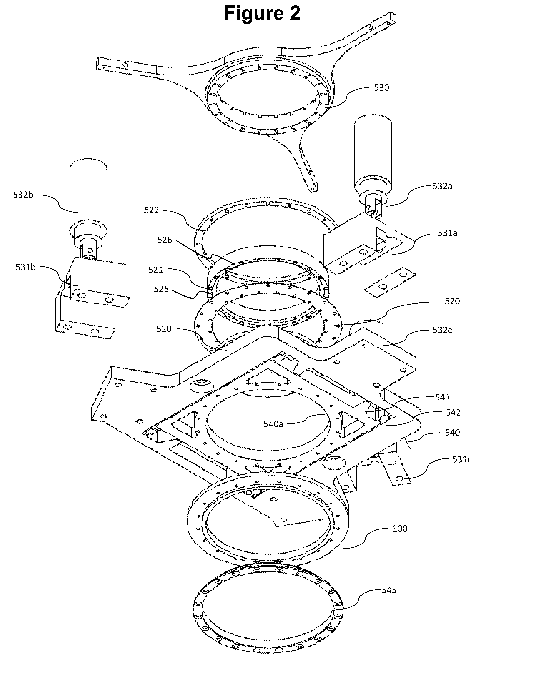
[0067]FIG. 1 illustrates the process flow steps to pickup semiconductor elements 20 from a donor substrate using a vacuum coupled tool apparatus. First the stamp is brought into close proximity (i.e. within 35 (FIG. 1A). After precise optical alignment of the stamp 100 to the donor substrate 30, the tool apparatus micro-chamber 550 is pressurized. The gas pressure induces a uniform pressure on the stamp backing top surface 40 and brings a stamp transfer surface 72 having relief features or protrusions 74, such as stamp printing posts, into conformal contact with semiconductor elements 20, illustrated as an array of semiconductor elements, defined on the top surface 35 of the donor substrate 30 (FIG. 1B). A passage 523 traverses from external surface 506 to internal surface 507 of top plate 505. The micro-chamber inlet port 522 seals microchamber 550, and a linear actuator is then energized to quickly lift the top plate 505, including an optically-transpa...

example 2

Composite Stamps

[0073]FIG. 8 provides a schematic cross-sectional view of an exemplary reinforced composite stamp 100, such as a stamp for use with any of the tool apparatuses provided herein. As shown in FIG. 8, the composite stamp comprises a deformable layer 70, a reinforcement layer 120, and a stiff support layer 150. An array of relief features 105 are defined on the external surface 80 of the deformable layer 70 to facilitate selective transfer of printed structures, such as semiconductor elements. Array of relief features 105 may comprise a relief pattern providing selective printing or patterning functionality. External surface 80 is the surface of deformable layer 70 configured such that it is that is capable of contacting donor or target substrates for dry-transfer printing processes, for example providing a contact surface, printing surface or receiving surface of stamp 100 for dry transfer contact printing. The deformable layer 70 also has an internal surface 75 that fac...

example 3

Shear Offset

[0100]FIG. 9 illustrates an embodiment where a second actuator 601 provides the capability of shear-offset printing, such as shear-offset printing of any of the tool apparatuses and / or composite stamps provided herein. In particular, actuator 601 is operationally connected to the base plate assembly 540 for generating stamp 100 motion in a direction that is substantially parallel to the plane of the transfer surface, as indicated by the direction of the arrow. More particularly, a composite stamp, such as any of the composite stamps disclosed in Ser. No. 12 / 177,963, filed Aug. 29, 2008, is connected to a print tool head, such as a base plate540. Further detail of tool head is provided in Ser. No. 12 / 177,963, which is hereby specifically incorporated by reference for the composite stamps, devices for holding the composite stamps and printing processes, for example. A reinforced composite stamp 100, such as disclosed in Ser. No. 12 / 177,963, is made of a stiff backplane lay...


PUM

PropertyMeasurementUnit
Timeaaaaaaaaaa
Pressureaaaaaaaaaa
Pressureaaaaaaaaaa

Abstract

Provided are an optimized tool apparatus and methods for dry transfer printing of semiconductor elements with high yield and good placement accuracy. The tool apparatus comprises a vacuum coupled fast peel apparatus that provides high pickup yield of the semiconductor elements. In an aspect, this vacuum coupled apparatus provides high pickup rates during pickup of the semiconductor elements from a donor/source wafer. Provided is a tool apparatus for dry transfer printing with a reinforced composite stamp having a thin glass-backing. The tool apparatus also comprises a pressure regulated micro-chamber which provides precise control of a composite stamp lamination and de-lamination. In an aspect, the micro-chamber has an internal cavity volume that is variably controlled, thereby providing precise control of the force on the stamp, and corresponding separation velocity, and improved semiconductor element pick-up and/or placement.

Description

STATEMENT REGARDING FEDERALLY SPONSORED RESEARCH OR DEVELOPMENT[0001]This invention was made, at least in part, with United States governmental support awarded by National Science Foundation Grant IIP-0712017. The United States Government has certain rights in this invention.BACKGROUND OF THE INVENTION[0002]Provided herein are devices and processes for transfer printing of semiconductors. More specifically the devices relate to a tool apparatus for transfer printing semiconductor elements with high transfer printing yield and placement accuracy.[0003]Semiconductor chip or die automated assembly equipments typically rely on the use of vacuum operated placement heads often referred to as vacuum grippers or pick-and-place tools. In their simplest embodiment, these placement heads typically consist of an open ended cylinder having a drilled nozzle surface which seals to the die to accomplish physical attachment. Semiconductor chips or die which are ultra thin, fragile, or too small cann...

Claims


Application Information

Patent Timeline
IPC IPC(8): B28B11/08
CPCH01L24/74G03F7/0002H01L2924/12041H01L21/187H01L21/67092H01L21/67282H01L2224/80H01L2924/01013H01L2924/0102H01L2924/01029H01L2924/01032H01L2924/01082H01L2924/10329H01L2924/10336H01L2924/10349H01L2924/14H01L2924/01005H01L2924/01006H01L2924/01019H01L2924/01023H01L2924/01033H01L2924/01047H01L2924/01067H01L2924/01075H01L2924/01322B82Y10/00B82Y40/00H01L2924/00H01L21/0274H01L24/80
Inventor MENARD, ETIENNE
Owner X DISPLAY CO TECH LTD
Why Eureka
Try Eureka