Field emission display

Inactive Publication Date: 2011-01-27
UVIS LIGHT
View PDF3 Cites 7 Cited by
  • Summary
  • Abstract
  • Description
  • Claims
  • Application Information

AI Technical Summary

Benefits of technology

[0013]Due to the height alignment characteristics of the nanostructures it can be possible to increase the lifetime of the field emission arrangement in which the field emission electrode according to the present invention is arranged, as there will be less of the nanostructures that will be non-height-aligned. The non-height-alignment present in a prior art field emission electrode led to a concentration of electron emission at the sections where the nanostructures are “extending closer” to an electron receptor adapted to receive electrons emitted by the field emission electrode. Furthermore, by not having to “height align” the nanostructures using an expensive prior art etching, grinding, or similar method step, it is possible to achieve a less expensive end product.
[0017]Preferably, the electrical insulation is selected from a group comprising an insulator, a semi-insulator, or a poor insulator. Different types of insulating compounds can be used, such as for example a polymer, a resin, rubber or silicone, for example having different flexibility and / or elasticity. However, other compound are possible. By means of a low temperature growth method it is possible to expand the selection of insulator materials as heat during the growth will not be a great problem. The insulating compound can thus be allowed to depend on desired characteristics for the field emission electrode.
[0018]In an alternative embodiment of the invention, the method further comprises the step of etching the exposed first end of the nanostructures. By etching the exposed first end of the nanostructures, it is possible to achieve sharp tips which will further enhance the emission of electrons.
[0021]This aspect of the invention provides similar advantages as according to the above discussed method for manufacturing of a field emission display, including for example increased lifetime of the filed emission display, for example due to the fact that there will be less of the nanostructures that will be non-height-aligned. Furthermore, by not having to height align the nanostructures using an expensive etching, grinding, or similar method step, it is possible to provide a less expensive end product. The field emission display is preferably manufactured using the method according to the present invention

Problems solved by technology

However, using the disclosed method for forming the electrode does not provide an accurate alignment of the height of the carbon tubes constituting the electrode, as the carbon tubes are allowed to grow independently of each other, thus resulting in carbon tubes having different height.
Different height of the independent carbon tubes leads to problems with obtaining homogeneous and stable electron emission, and for achieving a high current density.
Including additional processing steps for aligning the height of the plurality of carbon tubes would not be desirable as such processing steps would lead to an expensive end product.

Method used


Image

  • Field emission display
  • Field emission display
  • Field emission display

Examples


Embodiment Construction

[0027]The present invention will now be described more fully hereinafter with reference to the accompanying drawings, in which currently preferred embodiments of the invention are shown. This invention may, however, be embodied in many different forms and should not be construed as limited to the embodiments set forth herein; rather, these embodiments are provided for thoroughness and completeness, and fully convey the scope of the invention to the skilled addressee. Like reference characters refer to like elements throughout.

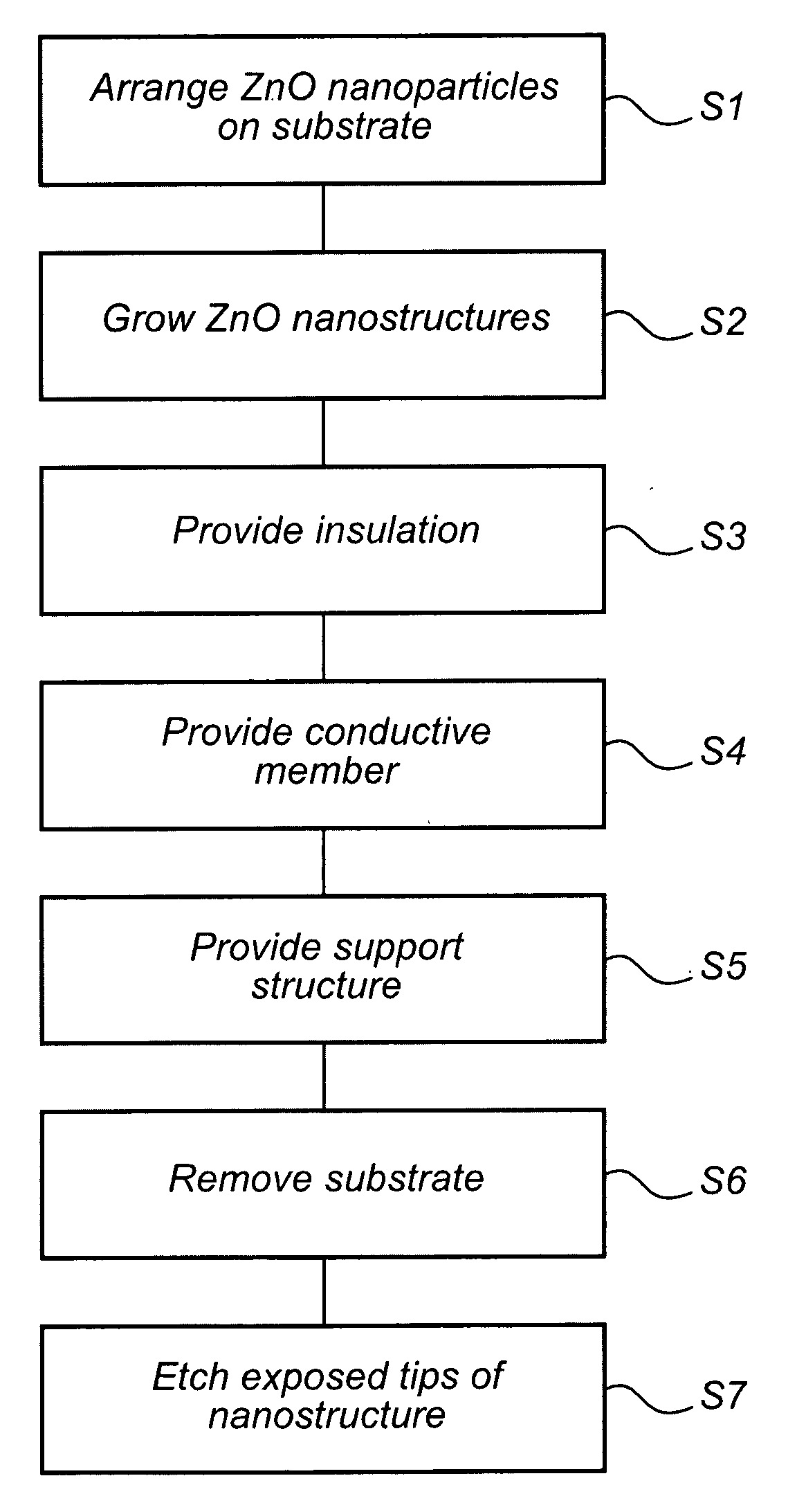
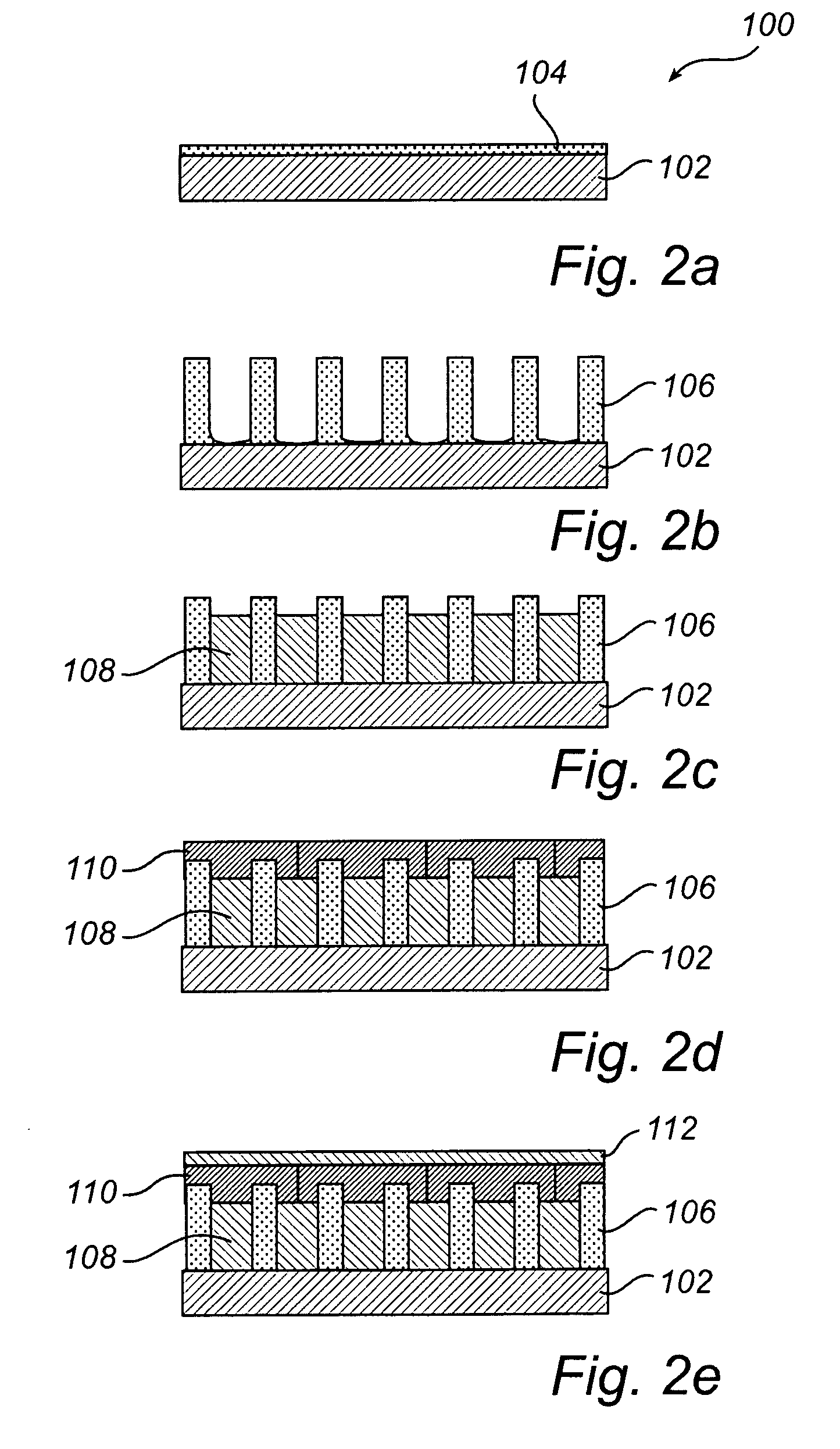
[0028]Referring now to the drawings and to FIG. 1 in particular, there is depicted a flowchart illustrating the method steps of manufacturing a field emission electrode 100 usable in a field emission display according to the present invention. Parallel to FIG. 1, FIGS. 2a-2g visualize the provision of a field emission electrode 100 during the corresponding manufacturing steps illustrated in FIG. 1. Thus parallel references will be given to FIGS. 1 and 2a-2g.

[0...


PUM


Abstract

The present invention relates to a method for the manufacturing of a field-emission display (300), comprising the steps of arranging an electron-emission receptor (302) in an evacuated chamber, arranging a wavelength converting material (304) in the vicinity of the electron-emission receptor, and arranging an electron-emission source (100) in the evacuated chamber, the electron-emission source adapted to emit electrons towards the electron-emission receptor, wherein the electron-emission source is formed by providing a substrate, forming a plurality of ZnO-nanostructures on the substrate, wherein the ZnO-nanostructures each have a first end and a second end, and the first end is connected to the substrate, arranging an electrical insulation to electrically insulate the ZnO-nanostructures from each other, connecting an electrical conductive member to the second end of a selection of the ZnO-nanostructures, arranging a support structure onto of the electrical conductive member, and removing the substrate, thereby exposing the first end of the ZnO-nano structures. Advantages with the invention include for example increased lifetime of the field-emission display as there will be a smaller sections of the nanostructures that will be non-height-aligned. Furthermore, by not having to height align the nanostructures using an expensive etching, grinding, or similar method step, it is possible to achieve a less expensive end product. The present invention also relates to a corresponding field-emission display.

Description

PRIORITY STATEMENT[0001]This application is the national phase under 35 U.S.C. §371 of PCT International Application No. PCT / EP2008 / 010831 which has an International filing date of Dec. 18, 2008, which designates the United States of America, and which claims priority on European patent application number 08150191.8 filed Jan. 11, 2008, the entire contents of each of which are hereby incorporated herein by reference.FIELD OF THE INVENTION[0002]The present invention relates to a method for the manufacturing of a field emission display. The present invention also relates to a corresponding field emission display.DESCRIPTION OF THE RELATED ART[0003]Recently, there has been an aggressive development of new types of flat panel displays for use in conjunction with various electronic devices. The main focus is currently on liquid crystal displays (LCDs), plasma display panels (PDPs), and organic light-emitting diode displays (OLED displays). However, another promising approach is the use o...

Claims


Application Information

Patent Timeline
IPC IPC(8): H01J1/62H01J9/02
CPCH01J1/304H01J9/025H01J2209/0223H01J2201/30496H01J31/127
Inventor HU, QIU-HONGKOMITOV, LATCHEZAR
Owner UVIS LIGHT
Why Eureka
Try Eureka