Semiconductor device

a semiconductor and active matrix technology, applied in static indicating devices, instruments, electroluminescent light sources, etc., can solve the problems of increasing power consumption, distorted scan line selection signals, and long so as to shorten rising time and falling time, reduce power consumption, and suppress signal distortion

Inactive Publication Date: 2011-01-27
SEMICON ENERGY LAB CO LTD
View PDF101 Cites 25 Cited by
  • Summary
  • Abstract
  • Description
  • Claims
  • Application Information

AI Technical Summary

Benefits of technology

[0012]An embodiment of this invention enables a signal with sufficient amplitude to be supplied to a scan line by bootstrap operation. Further, an embodiment of this invention can suppress distortion of a signal and shorten a rising time and a falling time. Furthermore, an embodiment of this invention does not need to have a power supply voltage which is higher than the voltage of an input signal, which results in low power consumption driving.

Problems solved by technology

At that time, Vgs of the transistor sometimes becomes small in accordance with a change of the potential of the other of the source and drain electrodes of the transistor, so that the scan line selection signal is often distorted and a rising time and a falling time often become long.
In order to solve the above problem, a signal with higher amplitude than an output signal of the scan line driver circuit or a power supply voltage is additionally needed but it causes an increase in power consumption.

Method used


Image

  • Semiconductor device
  • Semiconductor device
  • Semiconductor device

Examples


embodiment 1

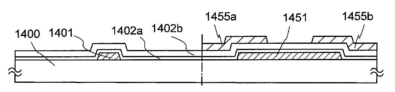
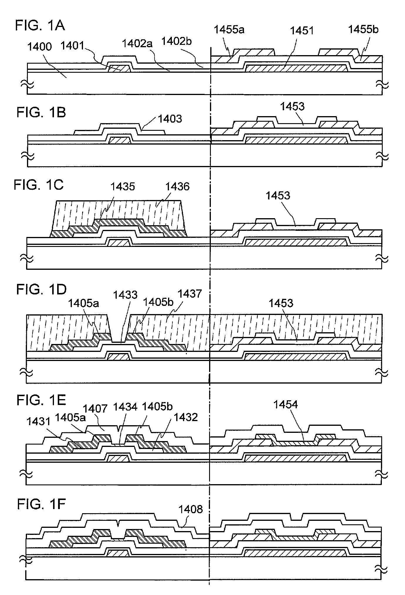
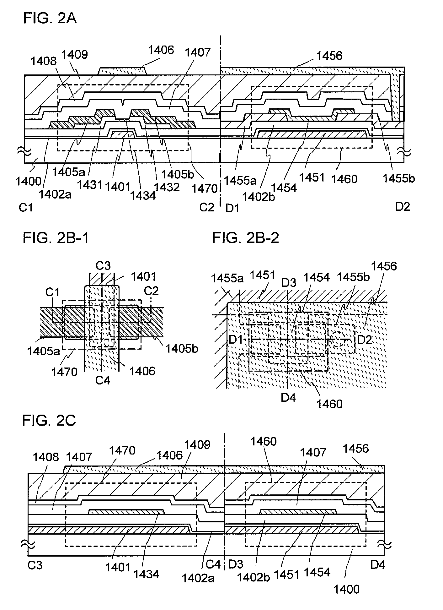
[0034]A semiconductor device and a manufacturing method of the semiconductor device will be described with reference to FIGS. 1A to 1F and FIGS. 2A, 2B-1, 2B-2, and 2C. FIG. 2A illustrates an example of a cross-sectional structure of two thin film transistors which have different structures from each other and are formed over the same substrate. FIG. 2A illustrates a thin film transistor 1470 of a channel-etched type which is one of bottom gate structures and a thin film transistor 1460 of a bottom-contacted type (an inverted coplanar type) which is one of bottom gate structures.

[0035]FIG. 2B-1 is a plan view of the channel-etched thin film transistor 1470 provided in a driver circuit. FIG. 2A is a cross-sectional view taken along line C1-C2 in FIG. 2B-1. In addition, FIG. 2C is a cross-sectional view taken along line C3-C4 in FIG. 2B-1.

[0036]The thin film transistor 1470 provided in the driver circuit is a channel-etched thin film transistor and includes a gate electrode layer 1401...

embodiment 2

[0109]One embodiment of a semiconductor device and a manufacturing method thereof will be described with reference to FIGS. 3A-1, 3A-2, 3B, and 3C, FIGS. 4A to 4E, and FIGS. 5A to 5E.

[0110]FIGS. 3A-1, 3A-2, 3B, and 3C illustrate an example of a plan view and a cross-sectional view of two thin film transistors which have different structures from each other and which are formed over the same substrate. FIGS. 3A-1, 3A-2, 3B, and 3C illustrate a thin film transistor 2410 of a channel-etched type which is one of bottom gate structures and a thin film transistor 2420 of a channel-protection type (also referred to as a channel stop type) which is one of bottom gate structures. The thin film transistor 2410 and the thin film transistor 2420 can be referred to as inverted staggered thin film transistors.

[0111]FIG. 3A-1 is a plan view of the channel-etched thin film transistor 2410 provided in a driver circuit. FIG. 3B is a cross-sectional view taken along line C1-C2 in FIG. 3A-1.

[0112]FIG. ...

embodiment 3

[0179]This embodiment describes an example of a semiconductor device in which a plurality of signals can be obtained from one signal. Here, the case where three signals can be obtained from one signal is described for example, this embodiment is not limited thereto. A various cases are acceptable as long as two or more signals can be obtained from one signal.

[0180]First, a structure of the semiconductor device of this embodiment will be described with reference to FIG. 6A.

[0181]A circuit 100 includes a circuit 110, a circuit 120, and a circuit 130. The circuit 110 includes a transistor 111 corresponding to a scan line switching element, a circuit 112, and a capacitor 114. The circuit 120 includes a transistor 121 corresponding to a scan line switching element, a circuit 122, and a capacitor 124. The circuit 130 includes a transistor 131 corresponding to a scan line switching element, a circuit 132, and a capacitor 134. A signal IN, a signal CK1, a signal CK2, a signal CK3, a signal ...


PUM


Abstract

It is an object to provide a semiconductor device which can supply a signal with sufficient amplitude to a scan line while power consumption is kept small. Further, it is an object to provide a semiconductor device which can suppress distortion of a signal supplied to the scan line and shorten a rising time and a falling time while power consumption is kept small. A semiconductor device which includes a plurality of pixels each including a display element and at least one first transistor and a scan line driver circuit supplying a signal for selecting the plurality of pixels to a scan line. A light-transmitting conductive layer is used for a pixel electrode layer of the display element, a gate electrode layer of the first transistor, source and drain electrode layers of the first transistor, and the scan line. The scan line driver circuit includes a second transistor and a capacitor for holding a voltage between a gate electrode layer of the second transistor and a source electrode layer of the second transistor. The source electrode of the second transistor is connected to the scan line.

Description

TECHNICAL FIELD[0001]This invention is related to an active matrix semiconductor device.BACKGROUND ART[0002]In an active matrix display device, a plurality of scan lines are led to intersect with a plurality of signal lines in a row direction and a column direction, and pixels each including a transistor, a pixel electrode, and a storage capacitor are provided at the intersections. The pixels are controlled by the plurality of scan lines which sequentially drives the pixels and the plurality of signal lines which supplies display signals to pixel electrodes. The scan line is connected to a scan line driver circuit for controlling the scan line. The signal line is connected to a signal line driver circuit for controlling the signal line. In order to control a plurality of pixels sequentially, the scan line driver circuit includes as many output terminals as the scan lines. The signal line driver circuit includes as many output terminals as the signal lines.[0003]Note that, in recent ...

Claims


Application Information

Patent Timeline
Patent Type & Authority Applications(United States)
IPC IPC(8): G09G5/02H05B44/00
CPCG09G3/3266G09G3/344G09G3/3677H01L27/1225G11C19/184H01L27/1251H01L28/40G09G2310/0267H01L27/124H01L27/1255H01L27/1214G09G2300/0809G09G2310/0213
Inventor UMEZAKI, ATSUSHIARASAWA, RYO
Owner SEMICON ENERGY LAB CO LTD
Why Eureka
Try Eureka