

IC Test Substrate for Testing Various Signals
a technology of test substrate and signal, applied in the direction of electronic circuit testing, measurement devices, instruments, etc., can solve the problems of insufficient power source, inability to exclude ssn, and too high target impedance, so as to ensure the integrity of power supply and ensure the practicability of products
- Summary
- Abstract
- Description
- Claims
- Application Information
AI Technical Summary
Benefits of technology
Problems solved by technology
Method used
Image

Examples
Embodiment Construction
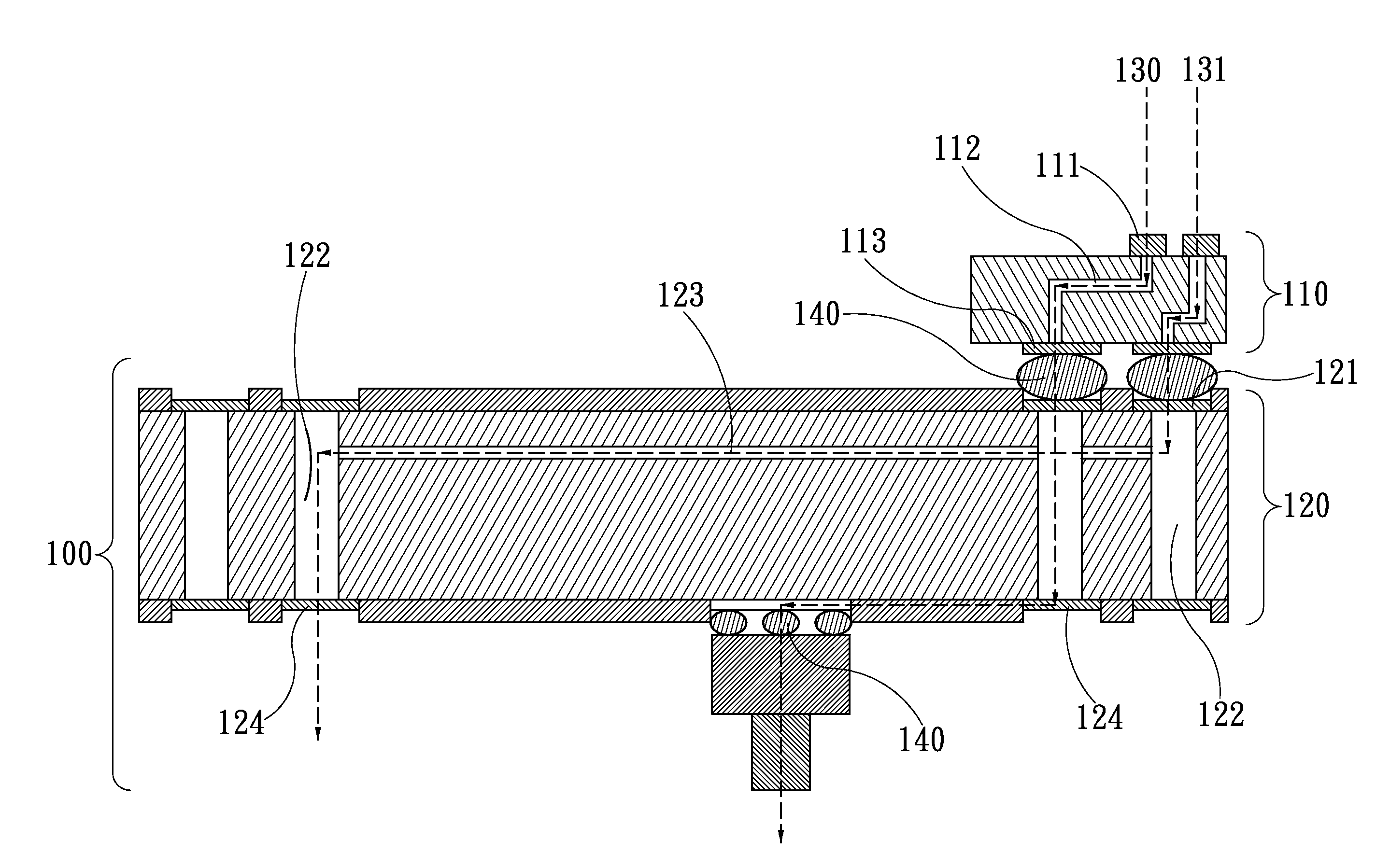
[0021]The present invention provides a scheme of a multi-functional IC test substrate. The combination of flexible and rigid PCB is formed of multiple layers of flexible PCB and multiple layers of rigid PCB. On the multiple layer flexible PCB, the signal, power and ground circuits are formed, wherein signals are communicated with a plurality of transmission wires and a plurality of through holes, and DUT signals are transmitted from the flexible PCB to an external probe card. On the multiple layered rigid PCB, the signal, power and ground circuits are formed, and signals are communicated with a plurality of transmission wires and a plurality of through holes through the substrate. The DUT signals are transmitted to an external probe card via BGA surface too, while the test signals are conducted by the metal conductor and the through holes so as to perform signal transmission.
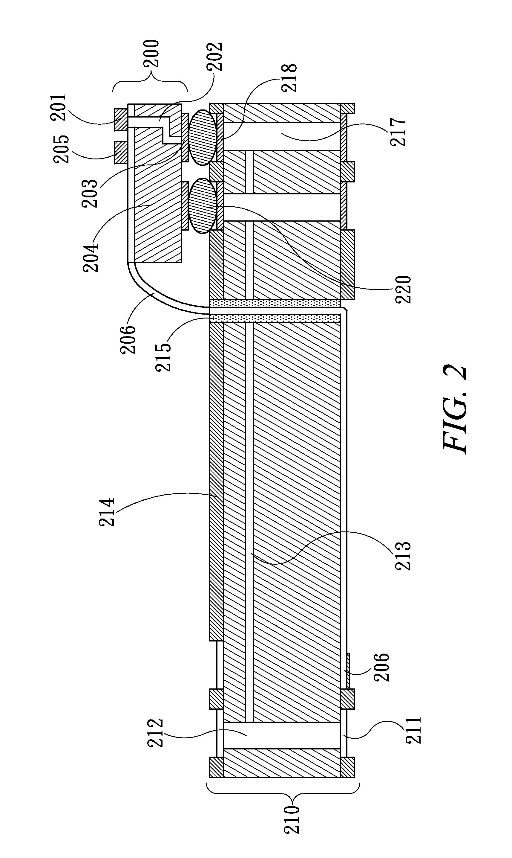
[0022]Referring to FIG. 2, the combined flexible and rigid PCB is applicable in two respects. The first one i...
PUM
 Abstract
Description
Claims
Application Information