Nanomesh SRAM Cell

a static random access memory and nanowire technology, applied in the field of nanowire-based static random access memory (sram) devices, can solve problems such as adversely affecting the performance of the completed devi

Inactive Publication Date: 2011-02-10
GLOBALFOUNDRIES INC
View PDF13 Cites 139 Cited by
  • Summary
  • Abstract
  • Description
  • Claims
  • Application Information

AI Technical Summary

Problems solved by technology

However, since features involved in the active area definition and gate definition are not all the same size and / or orientation, these features are prone to lithography, etching and other process variations.
Variations can adversely affect the performance of the completed device.

Method used


Image

  • Nanomesh SRAM Cell
  • Nanomesh SRAM Cell
  • Nanomesh SRAM Cell

Examples


Embodiment Construction

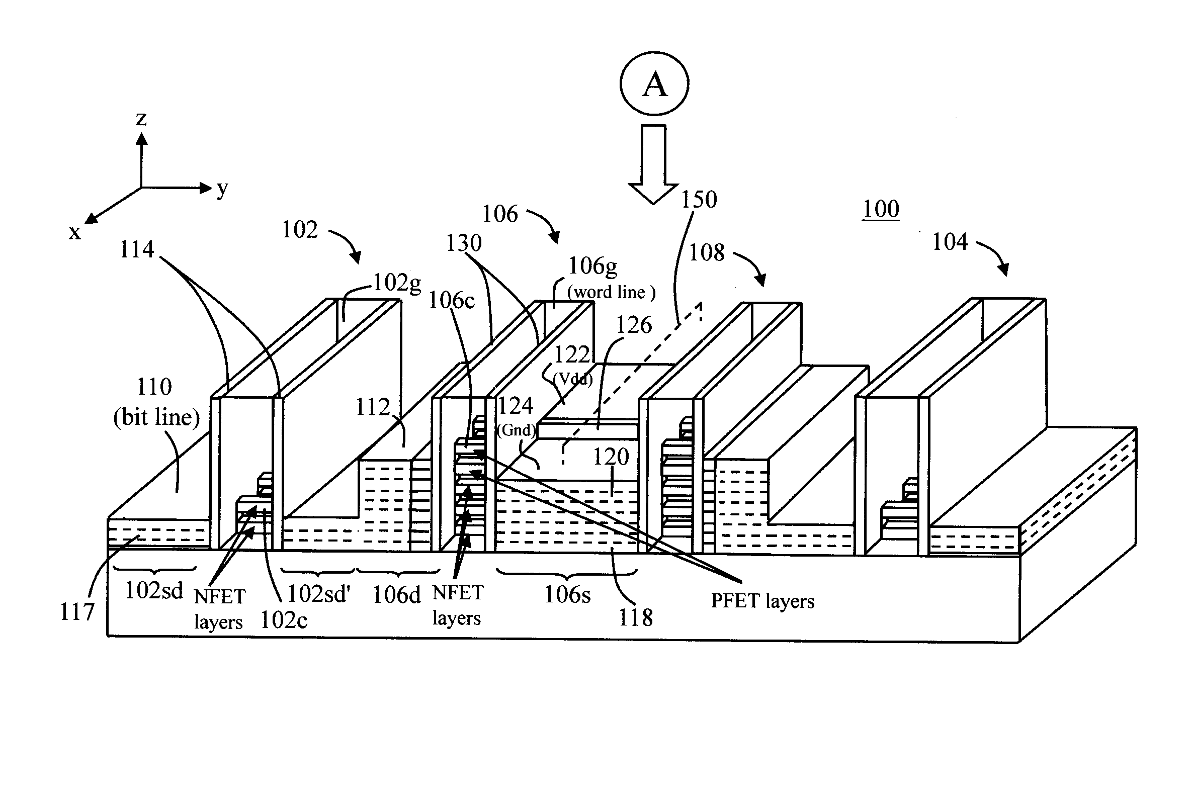
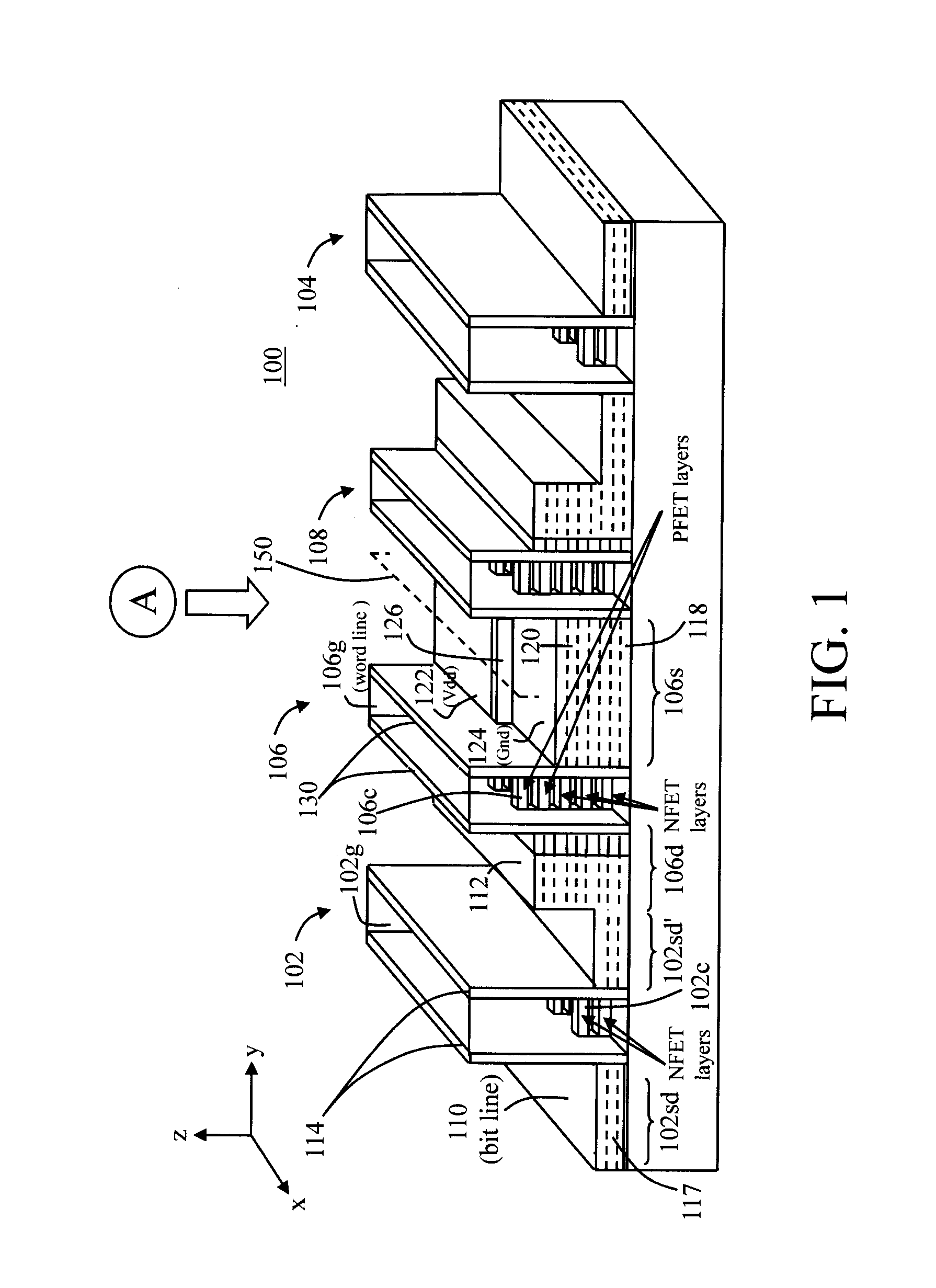
FIG. 1 is a three-dimensional cross-sectional diagram illustrating exemplary static random access memory (SRAM) cell 100. The configuration shown is a 6T SRAM cell containing six nanowire mesh-based field-effect transistors (FETs), configured as a pair of pass gates and a pair of inverters, e.g., with the pair of inverters located in between and separating the pair of pass gates. The depiction of a six transistor (6T) SRAM cell is merely to provide an example by which to illustrate the present teachings. Namely, other cell designs, such as 8T and 10T configurations may be similarly configured and would be within the scope of the present teachings.

The two pass gates, i.e., pass gates 102 and 104, each comprise one nanowire mesh-based transistor (an n-channel FET (NFET) transistor), and the two inverters, i.e., inverters 106 and 108, each comprise two nanowire mesh-based transistors (an NFET / p-channel FET (PFET) pair of transistors). According to the exemplary embodiment depicted in F...


PUM


Abstract

Nanowire-based devices are provided. In one aspect, a SRAM cell includes at least one pair of pass gates and at least one pair of inverters formed adjacent to one another on a wafer. Each pass gate includes one or more device layers each having a source region, a drain region and a plurality of nanowire channels connecting the source region and the drain region and a gate common to each of the pass gate device layers surrounding the nanowire channels. Each inverter includes a plurality of device layers each having a source region, a drain region and a plurality of nanowire channels connecting the source region and the drain region and a gate common to each of the inverter device layers surrounding the nanowire channels.

Description

BACKGROUND OF THE INVENTION1. Field of the InventionThe present invention relates to nanowire-based devices, and more particularly, to nanowire-based static random access memory (SRAM) devices.2. Description of the Related ArtIn a static random access memory (SRAM) cell a combination of field-effect transistors (FETs) are used to store each bit. For example, in a six transistor (6T) SRAM design each cell contains six field-effect transistors (FETs). Other configurations vary the number of transistors, such as eight transistor (8T) and ten transistor (10T) SRAM.In typical SRAM design layouts, there are many non-linear edges involved in the active area and gate definition masks. In conventional complementary metal-oxide semiconductor (CMOS)-based fabrication processes, the SRAM design layout is adjusted to obtain the smallest cell size possible so as to increase layout density, and hence great care is taken in the mask generation. However, since features involved in the active area de...

Claims


Application Information

Patent Timeline
Patent Type & Authority Applications(United States)
IPC IPC(8): H01L27/11H01L29/66H01L21/8239
CPCB82Y10/00H01L21/84H01L27/0688Y10S977/938H01L27/1104H01L27/1203H01L27/11H10B10/00H10B10/12
Inventor CHANG, JOSEPHINECHANG, PAULGUILLORN, MICHAEL A.SLEIGHT, JEFFREY
Owner GLOBALFOUNDRIES INC
Why Eureka
Try Eureka