Semiconductor device and manufacturing method thereof

a technology of semiconductors and semiconductors, applied in non-linear optics, instruments, optics, etc., can solve the problems of small on/off ratio, capacity load increase, switching characteristics, etc., and achieve excellent electric characteristics and high reliability

Active Publication Date: 2011-02-10
SEMICON ENERGY LAB CO LTD
View PDF100 Cites 71 Cited by
  • Summary
  • Abstract
  • Description
  • Claims
  • Application Information

AI Technical Summary

Benefits of technology

[0052]A semiconductor device including a thin film transistor which uses an oxide semiconductor layer and has excellent electric characteristics and high reliability can be realized.

Problems solved by technology

However, in the case where the channel length (L) is shortened, a problem of switching characteristics such as small on / off ratio arises.
Further, there is a problem in that the capacity load increases when the channel width (W) is increased.

Method used


Image

  • Semiconductor device and manufacturing method thereof
  • Semiconductor device and manufacturing method thereof
  • Semiconductor device and manufacturing method thereof

Examples


embodiment 1

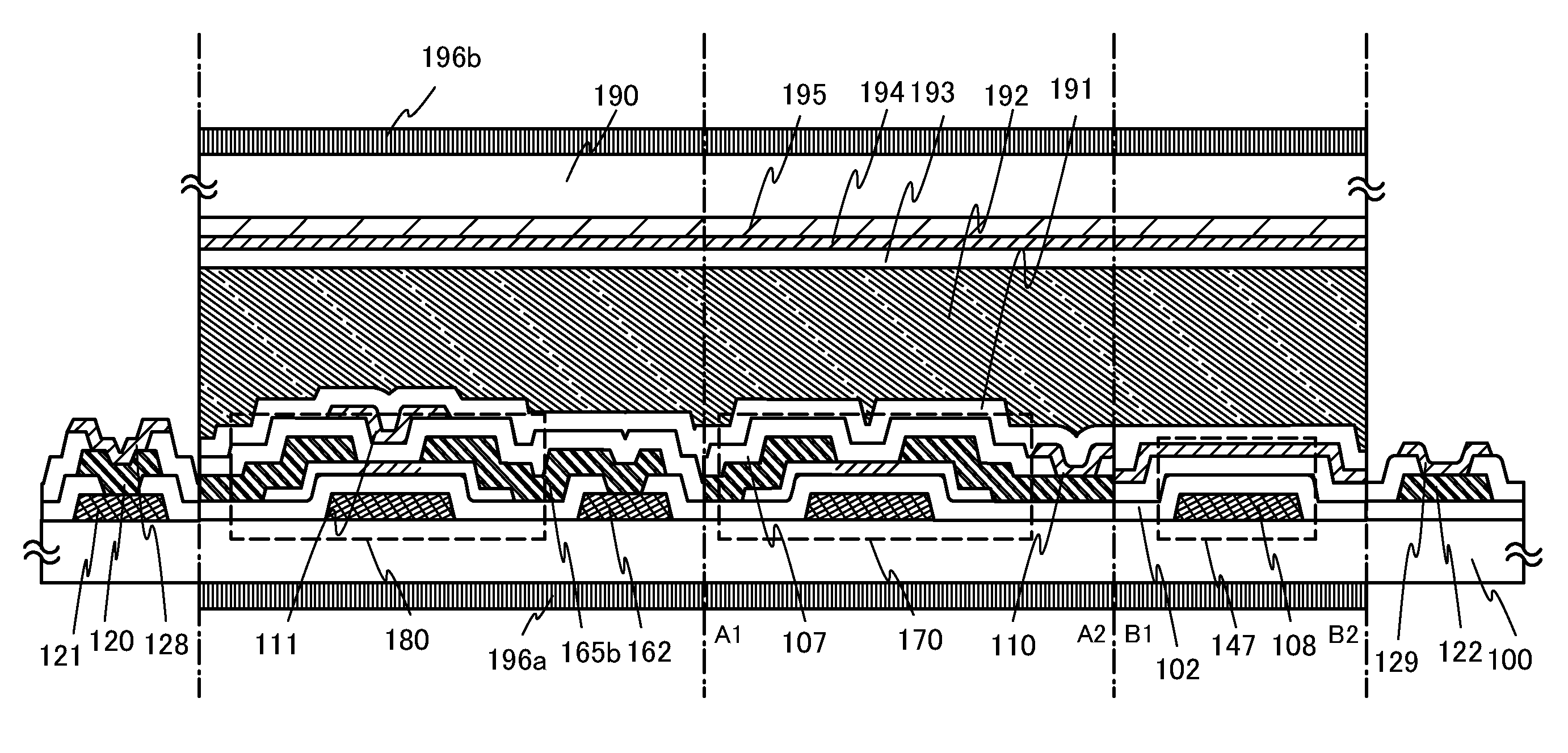
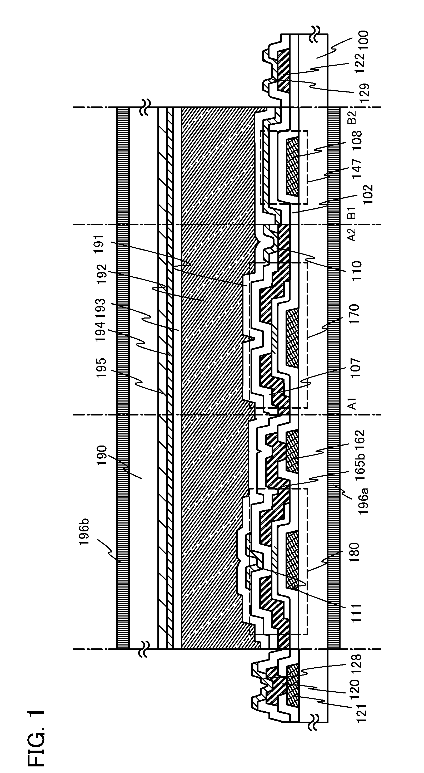
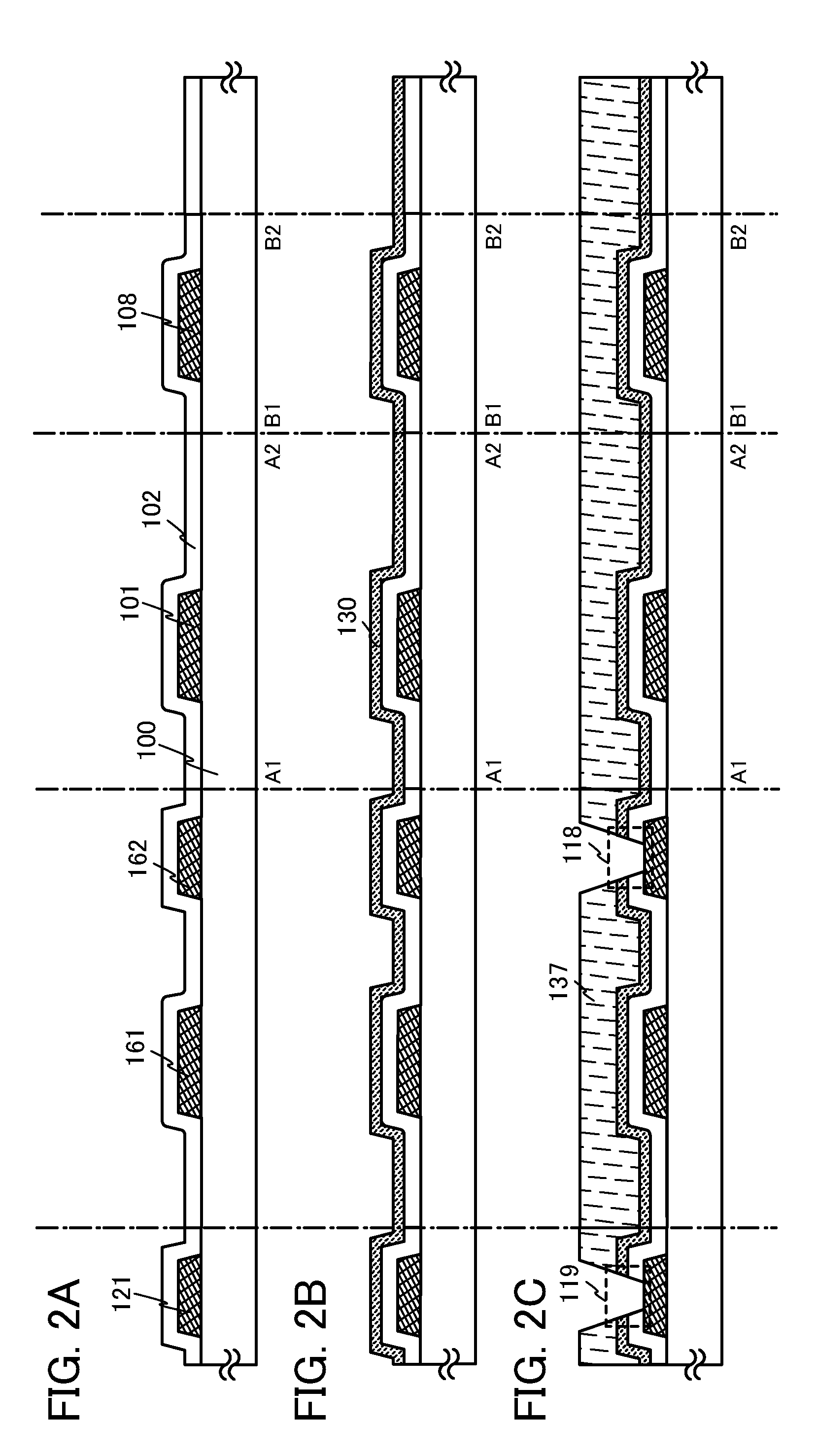
[0095]A manufacturing process of a semiconductor device including a thin film transistor will be described with reference to FIG. 1, FIGS. 2A to 2C, FIGS. 3A to 3C, FIGS. 4A to 4C, and FIG. 5.

[0096]A liquid crystal display device as a semiconductor device which is one embodiment of the present invention is illustrated in FIG. 1. In the liquid crystal display device in FIG. 1, a substrate 100 which is provided with a pixel portion including a thin film transistor 170 and a capacitor 147, a driver circuit portion including a thin film transistor 180, a pixel electrode layer 110, and an insulating layer 191 serving as an alignment film, and a counter substrate 190 which is provided with an insulating layer 193 serving as an alignment film, a counter electrode layer 194, and a coloring layer 195 serving as a color filter face each other with a liquid crystal layer 192 positioned between the substrates. The substrate 100 is provided with a polarizing plate (a layer including a polarizer,...

embodiment 2

[0196]In this embodiment, an example in which oxide conductive layers are provided as a source region and a drain region between the oxide semiconductor layer and the source and drain electrode layers in Embodiment 1 will be described with reference to FIGS. 6A to 6D and FIGS. 7A and 7B. Therefore, part of this embodiment can be performed in a manner similar to that of Embodiment 1, and repetitive description of the same portions as or portions having functions similar to those in Embodiment 1 and steps for manufacturing such portions will be omitted. Further, since the steps in FIGS. 6A to 6D and FIGS. 7A and 7B are the same as the steps in FIG. 1, FIGS. 2A to 2C, FIGS. 3A to 3C, FIGS. 4A to 4C, and FIG. 5 except some points, the same portions are denoted by the same reference numerals and the detailed description of the same portions will be omitted.

[0197]First, the steps up to the step of FIG. 3B in Embodiment 1 are performed in accordance with Embodiment 1. FIG. 6A is the same a...

embodiment 3

[0223]In this embodiment, another example in which oxide conductive layers are provided as a source region and a drain region between the oxide semiconductor layer and the source and drain electrode layers in Embodiment 1 or 2 will be described with reference to FIGS. 8A to 8D and FIGS. 9A and 9B. Therefore, part of this embodiment can be performed in a manner similar to that of Embodiment 1 or 2, and repetitive description of the same portions as or portions having functions similar to those in Embodiment 1 or 2 and steps for manufacturing such portions will be omitted. Further, since the steps in FIGS. 8A to 8D and FIGS. 9A and 9B are the same as the steps in FIG. 1, FIGS. 2A to 2C, FIGS. 3A to 3C, FIGS. 4A to 4C, FIG. 5, FIGS. 6A to 6D, and FIGS. 7A and 7B except some points, the same portions are denoted by the same reference numerals and the detailed description of the same portions will be omitted.

[0224]First, in accordance with Embodiment 1, a metal conductive film is formed ...


PUM

PropertyMeasurementUnit
strain pointaaaaaaaaaa
gate threshold voltageaaaaaaaaaa

Abstract

An object is to improve reliability of a semiconductor device. A semiconductor device including a driver circuit portion and a display portion (also referred to as a pixel portion) over the same substrate is provided. The driver circuit portion and the display portion include thin film transistors in which a semiconductor layer includes an oxide semiconductor; a first wiring; and a second wiring. The thin film transistors each include a source electrode layer and a drain electrode layer. In the thin film transistor in the driver circuit portion, the semiconductor layer is sandwiched between a gate electrode layer and a conductive layer. The first wiring and the second wiring are electrically connected to each other in an opening provided in a gate insulating film through an oxide conductive layer.

Description

BACKGROUND OF THE INVENTION[0001]1. Field of the Invention[0002]The present invention relates to a semiconductor device including an oxide semiconductor.[0003]In this specification, a semiconductor device means all types of devices which can function by utilizing semiconductor characteristics, and an electro-optical device such as a liquid crystal display device, a semiconductor circuit, and an electronic appliance are all semiconductor devices.[0004]2. Description of the Related Art[0005]In recent years, a technique for forming a thin film transistor (TFT) by using a semiconductor thin film (having a thickness of approximately several nanometers to several hundreds of nanometers) formed over a substrate having an insulating surface has attracted attention. Thin film transistors are applied to a wide range of electronic devices such as integrated circuits (ICs) and electro-optical devices, and thin film transistors that are used as switching elements in image display devices are, in...

Claims


Application Information

Patent Timeline
Patent Type & Authority Applications(United States)
IPC IPC(8): G02F1/136H01L27/12H01L21/34H01L21/84
CPCH01L27/124H01L27/1225H01L29/78648G02F1/136227G02F1/1368G02F1/133302G02F1/133357H01L29/78693G02F1/13306G02F1/133345G02F1/133528G02F1/1337G02F1/1339G02F1/13394G02F1/134336G02F1/13439G02F1/13454G02F1/136204G02F1/136286G02F2201/123G11C19/28H01L27/1255H01L27/127H01L27/1288H01L29/247H01L29/78618H01L29/78696
Inventor YAMAZAKI, SHUNPEISAKATA, JUNICHIROSAKAKURA, MASAYUKIOIKAWA, YOSHIAKIOKAZAKI, KENICHIMARUYAMA, HOTAKATSUBUKU, MASASHI
Owner SEMICON ENERGY LAB CO LTD
Why Eureka
Try Eureka