Microstructured Fiber End
a technology of microstructured fibers and end caps, applied in the field of microstructured fibers, can solve the problems of inability to achieve the effect of enhancing the transmission of light, poor adhesion of coatings to chalcogenide glass, and limited infrared materials,
- Summary
- Abstract
- Description
- Claims
- Application Information
AI Technical Summary
Benefits of technology
Problems solved by technology
Method used
Image
Examples
example 1
A study was conducted to investigate the effect of optical transmission efficiency as a result of forming motheye arrays directly on the terminal end surface of infrared multimode As2S3 optical fibers. The As2S3 optical fiber, having a core diameter of about 100 μm, a cladding diameter of about 180 μm transmitted light over a mid-infrared range of about 2 μm to about 5 μm.
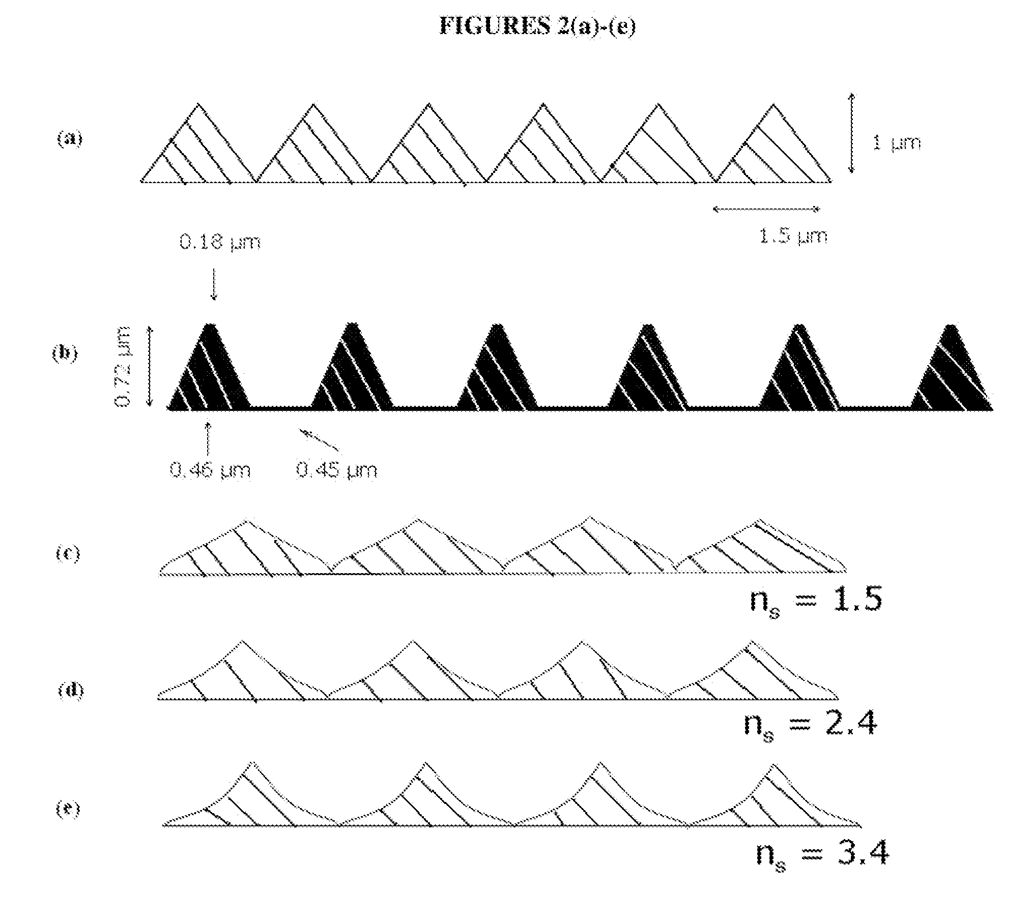
Three different micropatterns were evaluated in the study. Each microstructured array was imprinted onto the terminal end of three different As2S3 optical fibers using a direct stamping method. The method involved forming a template, which is known in the art as a shim, having the negative inverse microstructure pattern. The shims were designed using either TelAztec LLC's Rigorous Coupled-Wave Analysis (RCWA) software or a software using a second order approach to the effective medium theory. A first template, shown in FIG. 8(a), was fabricated from nickel and had a motheye array consisting of a collection of small...
example 2
A plurality of microstructures was formed on the terminal end of an As2S3 infrared optical fiber using the same method described in Example 1. An inverted negative micropattern including a plurality of pyramids was acid-etched onto a silicon wafer template. The template was then used to imprint pyramid shaped depressions having a depth of less than about 200 nm, as illustrated in FIG. 13(a)-13(c), onto the terminal end of the As2S3 fiber.
example 3
A study was conducted to determine the depth to which a microstructure may be imprinted on the terminal end of an As2S3 infrared optical fiber using the same method described in Example 1. As shown in FIG. 14(a)-14(b), a two dimensional microstructure array having protuberances with a height of about 10 to about 20 μm was found to be readily feasible.
PUM
 Abstract
Description
Claims
Application Information


