Method for driving touch panel

Active Publication Date: 2011-02-24
SEMICON ENERGY LAB CO LTD
View PDF34 Cites 17 Cited by
  • Summary
  • Abstract
  • Description
  • Claims
  • Application Information

AI Technical Summary

Benefits of technology

[0021]With one embodiment of the present invention, it is possible to provide a touch panel capable of high-speed imaging.
[0022]In addition, with one embodiment of the present invention, it is possible to provide a method for driving a touch panel capable of

Problems solved by technology

In the case where a portion different from the display portion has a personal authentication function, the

Method used


Image

  • Method for driving touch panel
  • Method for driving touch panel
  • Method for driving touch panel

Examples


Example

Embodiment 1

[0038]In this embodiment, a structure of a touch panel in one embodiment of the present invention and a driving method thereof are described with reference to FIG. 1, FIG. 2, FIG. 3, FIG. 4, FIG. 7, FIG. 10, and FIG. 11.

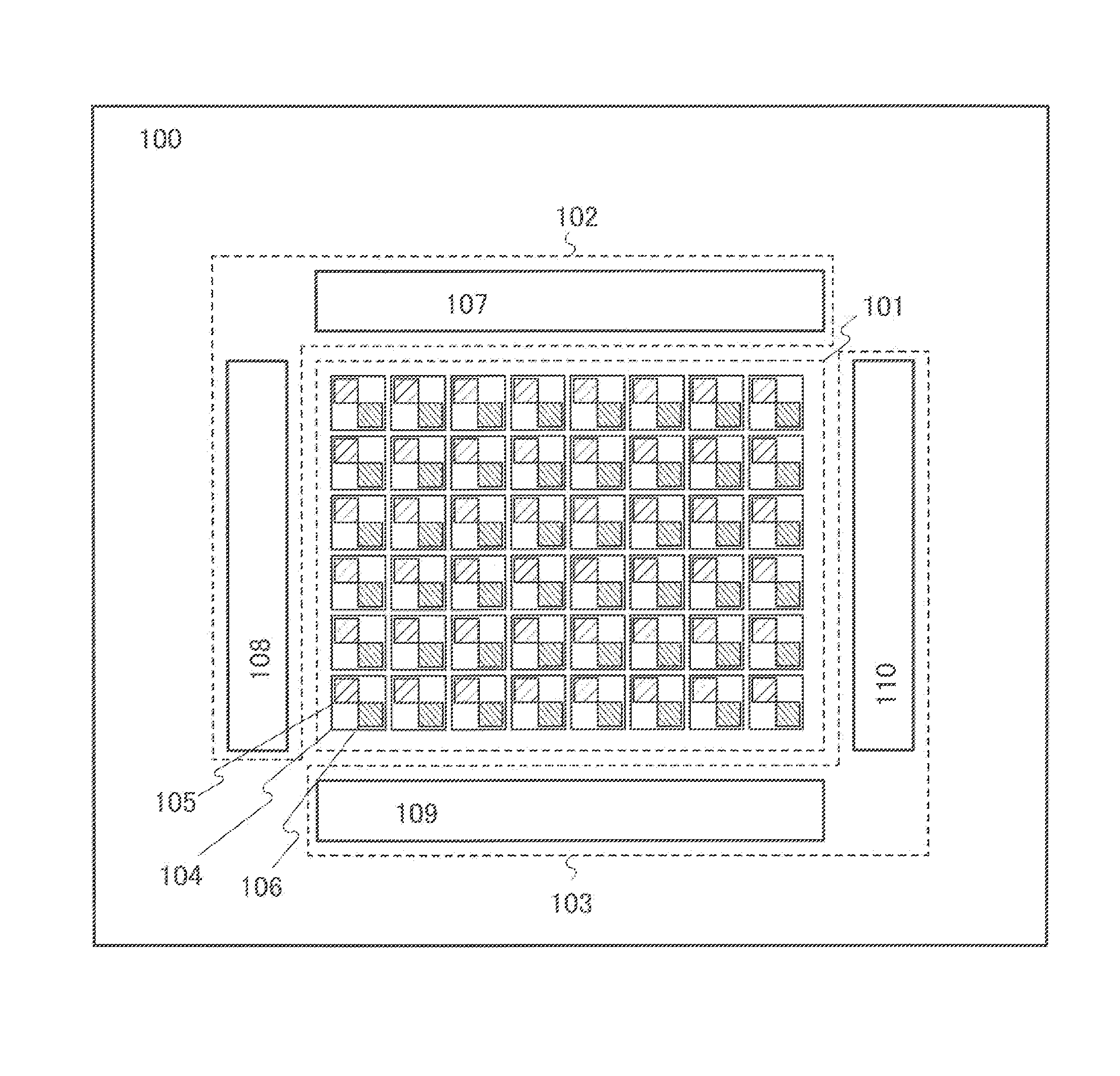
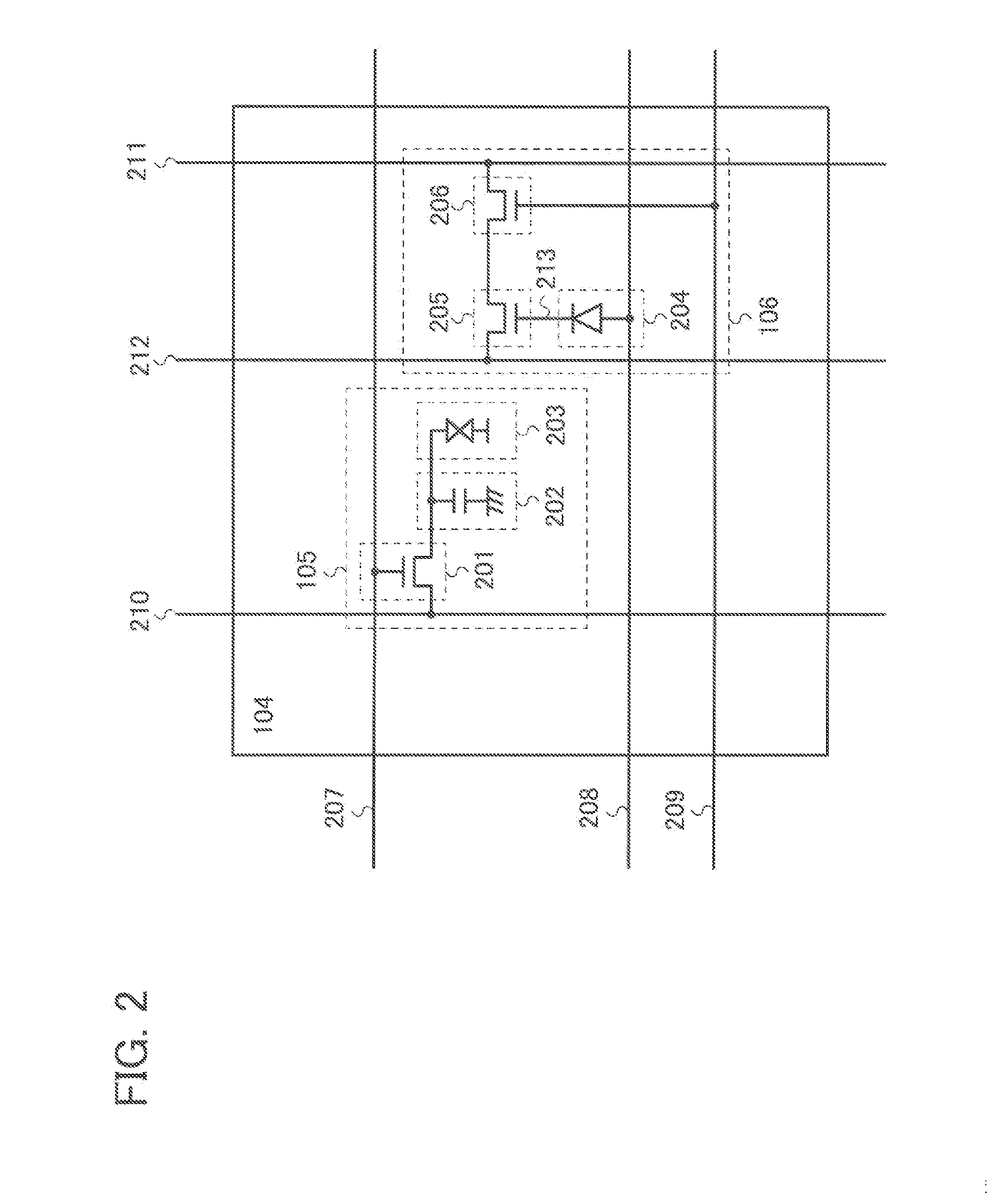
[0039]An example of a structure of a touch panel is described with reference to FIG. 1. A touch panel 100 includes a pixel circuit 101, a display element control circuit 102, and a photo sensor control circuit 103. The pixel circuit 101 includes a plurality of pixels 104 arranged in a matrix of rows and columns. Each of the pixels 104 includes a display element 105 and a photo sensor 106.

[0040]Each of the display elements 105 includes a thin film transistor (TFT), a storage capacitor, a liquid crystal element including a liquid crystal layer, and the like. The thin film transistor has a function of controlling injection or ejection of charge to / from the storage capacitor. The storage capacitor has a function of holding charge which corresponds to voltage ...

Example

Embodiment 2

[0081]In this embodiment, a structure of a touch panel in one embodiment of the present invention is described with reference to FIG. 5.

[0082]FIG. 5 illustrates an example of a cross-sectional view of the touch panel. In the touch panel illustrated in FIG. 5, a photodiode 502, a transistor 503, a storage capacitor 504, and a liquid crystal element 505 are formed over a substrate 501 (a TFT substrate) having an insulating surface.

[0083]The photodiode 502 and the storage capacitor 504 can be formed concurrently with the transistor 503 in a manufacturing process of the transistor 503. The photodiode 502 is a lateral-junction pin diode. A semiconductor film 506 included in the photo diode 502 has a region having p-type conductivity (a p-type layer), a region having i-type conductivity (an i-type layer), and a region having n-type conductivity (an n-type layer). Note that although the touch panel in which the photodiode 502 is a pin diode is shown in FIG. 5, the photodiode 50...

Example

Embodiment 3

[0098]In this embodiment, another structure of a touch panel in one embodiment of the present invention is described with reference to FIG. 6.

[0099]FIG. 6 illustrates an example of a cross-sectional view of the touch panel, which is different from that in Embodiment 2. In the touch panel illustrated in FIG. 6, a photodiode 602 differs from a photodiode 502 in FIG. 5 in having a shielding film 603 formed using a conductive film that is used for a gate electrode of a transistor 503. By providing the shielding film 603 in the photodiode 602, light from the backlight can be prevented from directly entering a region that has i-type conductivity (an i-type layer), and only light reflected by the object to be detected 521 can be efficiently detected.

[0100]In addition, in the case where the photodiode 602 serves as a lateral pin diode, a region that has p-type conductivity (a p-type layer) and a region that has n-type conductivity (an n-type layer) can be formed in a self-aligne...


PUM


Abstract

A touch panel includes a plurality of pixels each of which is provided with a photo sensor including a photodiode, a first transistor, and a second transistor. Each pixel performs first operation in which a potential of a photodiode reset signal line which is electrically connected to the photodiode is set so that a forward bias is applied to the photodiode, second operation in which a potential of a gate of the first transistor is changed by a photocurrent of the photodiode, and third operation in which a potential of a gate of the second transistor is changed and the photo sensor output signal line and a photo sensor reference signal line are brought into conduction through the first transistor and the second transistor so that the potential of the photo sensor output signal line is changed in accordance with the photocurrent.

Description

BACKGROUND OF THE INVENTION[0001]1. Field of the Invention[0002]The present invention relates to a touch panel including a photo sensor and a driving method thereof. In particular, the present invention relates to a touch panel including a plurality of pixels each of which is provided with a photo sensor and relates to a driving method thereof. Further, the invention relates to electronic devices including the touch panel.[0003]2. Description of the Related Art[0004]In recent years, a display device provided with a touch sensor has attracted attention. The display device provided with the touch sensor is called a touch panel a touch screen, and the like (hereinafter simply referred to as a “touch panel”). Examples of the touch sensor include a resistive touch sensor, a capacitance touch sensor, and an optical touch sensor, depending on its operation principle. In any of the sensors, when an object to be detected is in contact with a display device or in the vicinity of the display d...

Claims


Application Information

Patent Timeline
IPC IPC(8): G06F3/042
CPCG06F3/042G06F3/0304G06F3/0416
Inventor KUROKAWA, YOSHIYUKIIKEDA, TAKAYUKI
Owner SEMICON ENERGY LAB CO LTD
Why Eureka
Try Eureka