Method for Manufacturing a Resistive Switching Memory Cell Comprising a Nickel Oxide Layer Operable at Low-Power and Memory Cells Obtained Thereof

a nickel oxide layer and memory cell technology, applied in the field of non-volatile memory cells, can solve the problems of nio based reram memory cells, non-volatile memory technology will face severe scaling problems, and reduce the amount of charge, so as to improve the resistance of this high resistive state, improve the retention properties, and reduce the forming step voltage vforming

Active Publication Date: 2011-02-24
INTERUNIVERSITAIR MICRO ELECTRONICS CENT (IMEC VZW)
View PDF22 Cites 24 Cited by
  • Summary
  • Abstract
  • Description
  • Claims
  • Application Information

AI Technical Summary

Benefits of technology

[0015]It is an advantage of a metal oxide based ReRAM memory element according to the embodiments that it can operate at a low set and reset power.
[0016]It is an advantage that the reset current Ireset of unipolar resistive-switching non-volatile memory elements according to the embodiments, for resetting the memory element to a high resistive state, can be less than 100 uA, for example less than 50 uA. The resistivity of this high resistive state increases with temperature.
[0017]It is an advantage that the set voltage Vset of unipolar resistive-switching non-volatile memory elements according to the embodiments can be less than 1V.
[0018]It is an advantage of a metal oxide based ReRAM memory element according to the embodiments that it has a low forming step voltage Vforming, e.g. below 3 Volts.
[0019]It is an advantage of a metal oxide based ReRAM memory element and a method for operating such memory element according to the embodiments that it provides a reproducible filament formation and erasure.
[0020]It is an advantage of a metal oxide based ReRAM memory element according to the embodiments that it has better retention properties than prior art devices.

Problems solved by technology

It is expected that this type of non-volatile memory technology will face severe scaling problems beyond the 45 nm technology node due to fundamental physical limitations associated with this data storage mechanism as put forward in the International Technology Roadmap for Semiconductors (ITRS), “2005 edition, Process integration, Devices and Structures” as downscaling the memory cell dimensions inherently leads to a reduction of the amount of charge, representative for a value of the bit, that can be stored in the memory cell.
A major drawback of the state-of-the-art NiO based ReRAM memory cells is that they require high electro-forming voltage and reset current.

Method used


Image

  • Method for Manufacturing a Resistive Switching Memory Cell Comprising a Nickel Oxide Layer Operable at Low-Power and Memory Cells Obtained Thereof
  • Method for Manufacturing a Resistive Switching Memory Cell Comprising a Nickel Oxide Layer Operable at Low-Power and Memory Cells Obtained Thereof
  • Method for Manufacturing a Resistive Switching Memory Cell Comprising a Nickel Oxide Layer Operable at Low-Power and Memory Cells Obtained Thereof

Examples


Embodiment Construction

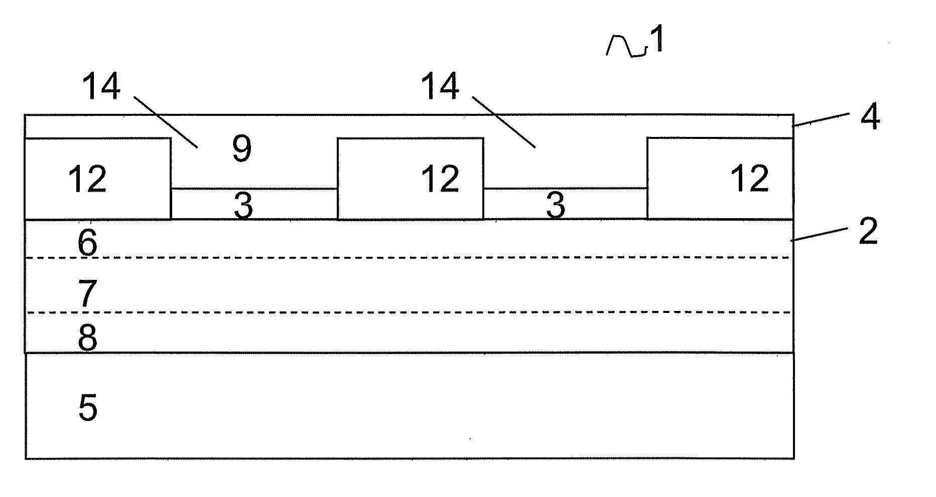
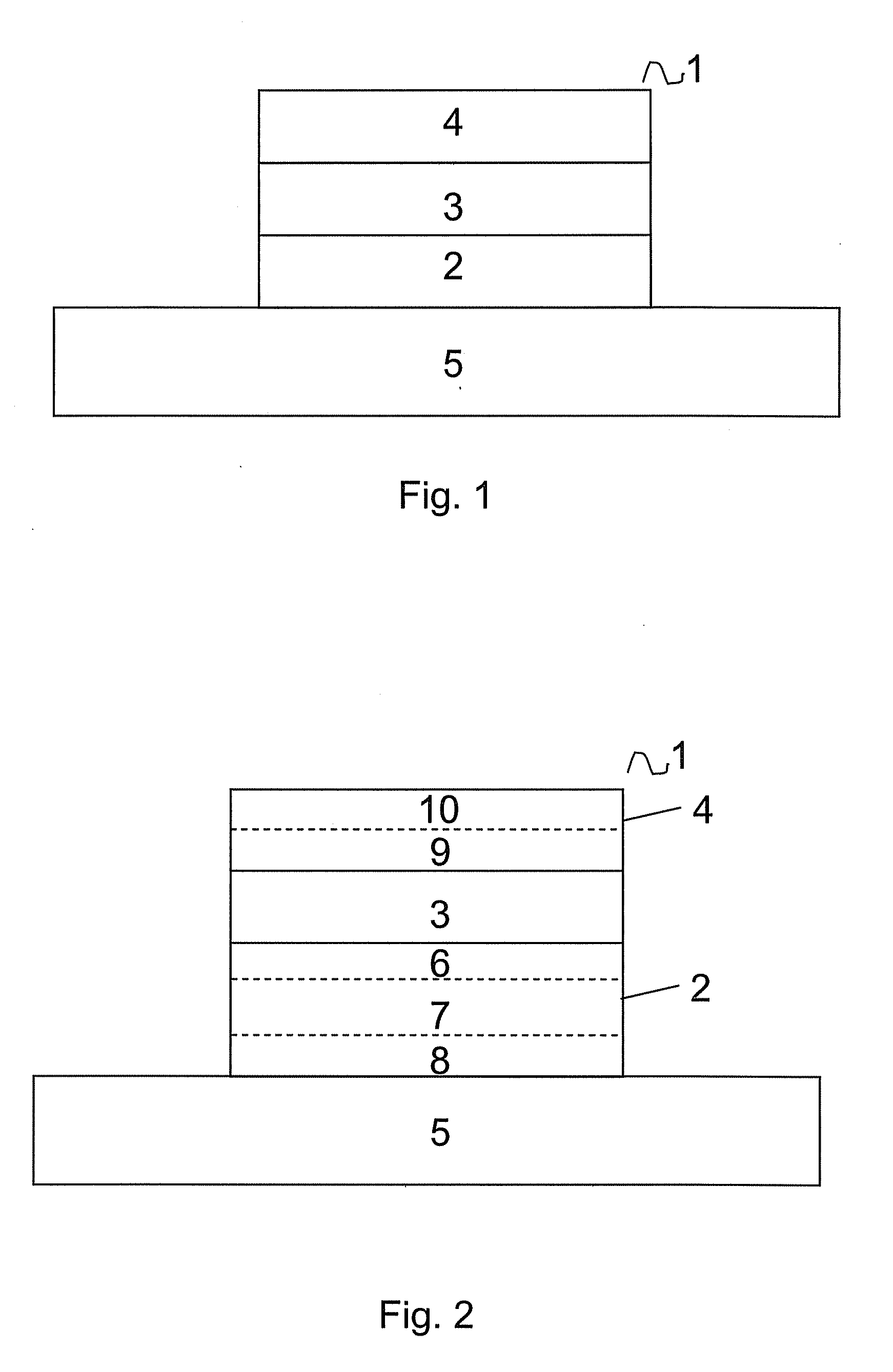
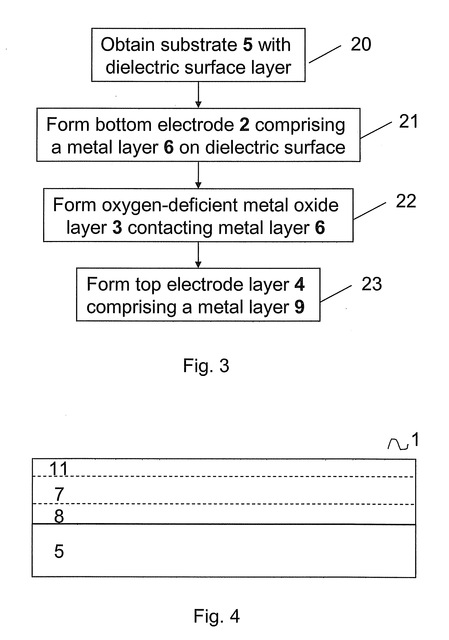
[0047]The present systems and methods will be described with respect to particular embodiments and with reference to certain drawings but the invention, as set forth in the claims, is not limited to those embodiments. The drawings described are only schematic and are non-limiting. In the drawings, the size of some of the elements may be exaggerated and not drawn on scale for illustrative purposes. The dimensions and the relative dimensions do not necessarily correspond to actual reductions to practice.

[0048]Moreover, the terms over, under, underneath and the like in the description and the claims are used for descriptive purposes and not necessarily for describing relative positions. It is to be understood that the terms so used are interchangeable under appropriate circumstances and that the embodiments described herein are capable of operation in other orientations than described or illustrated herein.

[0049]It is to be noticed that the term “comprising”, used in the claims, should...


PUM

PropertyMeasurementUnit
voltageaaaaaaaaaa
compliance currentaaaaaaaaaa
electro-forming voltageaaaaaaaaaa

Abstract

A resistive switching non-volatile memory element is disclosed comprising a resistive switching metal-oxide layer sandwiched between and in contact with a top electrode and a bottom electrode, the resistive switching metal oxide layer having a substantial isotropic non-stoichiometric metal-to-oxygen ratio. For example, the memory element may comprise a nickel oxide resistive switching layer sandwiched between and in contact with a nickel top electrode and a nickel bottom electrode whereby the ratio oxygen-to-nickel of the nickel oxide layer is between 0 and 0.85.

Description

CROSS-REFERENCE TO RELATED APPLICATIONS[0001]The present application claims priority to U.S. Provisional Patent Application No. 61 / 183,226 filed in the US Patent and Trademark Office on Jun. 2, 2009, the entire contents of which is incorporated herein by reference.BACKGROUND[0002]1. Field of the Invention[0003]The present disclosure relates to a non-volatile memory cell comprising a reversible resistance switching metal oxide layer, its resistance value being representative of the data stored in the memory cell.[0004]2. Description of the Related Art[0005]Today the Flash non-volatile memory (NVM) technology dominates the market of non-volatile memories. In a flash NVM memory charge is stored in a conductive or non-conductive charge storage layer incorporated in a MOSFET structure. It is expected that this type of non-volatile memory technology will face severe scaling problems beyond the 45 nm technology node due to fundamental physical limitations associated with this data storage ...

Claims


Application Information

Patent Timeline
Patent Type & Authority Applications(United States)
IPC IPC(8): G11C11/56H01L45/00H01L21/02
CPCG11C11/5614G11C13/0011G11C2213/34H01L45/146H01L45/1233H01L45/1253H01L45/08H10N70/24H10N70/826H10N70/841H10N70/8833
Inventor GOUX, LUDOVICREYES, JUDIT LISONIWOUTERS, DIRK
Owner INTERUNIVERSITAIR MICRO ELECTRONICS CENT (IMEC VZW)
Why Eureka
Try Eureka