Germanium layer polishing

a germanium layer and polishing technology, applied in the field of polishing germanium layers, can solve the problems of increasing the surface roughness of epitaxially grown germanium layers, affecting the polishing effect, so as to reduce the level of roughness and increase the removal rate

Active Publication Date: 2011-02-24
SOITEC SA
View PDF11 Cites 17 Cited by
  • Summary
  • Abstract
  • Description
  • Claims
  • Application Information

AI Technical Summary

Benefits of technology

[0011]It is an object of the invention to overcome the drawbacks mentioned above and to provide a solution for the polishing of germanium layers having an increased rate of removal while making it possible to further reduce the level of roughness present on the surface of germanium layers.
[0013]By using a polishing solution having an acidic pH during a first chemical-mechanical polishing step, a much higher rate of germanium removal is obtained than with a polishing solution conventionally used for this type of material, namely a solution having an alkaline pH. In the case of a germanium layer formed by heteroepitaxy, this first polishing step makes it possible initially to remove enough germanium in order to eliminate the surface defects due to the epitaxial growth of the germanium layer and to reduce the surface roughness in part. The second polishing step makes it possible to significantly reduce the microroughness and the macroroughness of the surface of the germanium layer, in particular the haze. After this second polishing step, the germanium layer has a surface roughness level compatible with bonding by molecular adhesion.
[0015]During the first polishing step, it is preferable to use a “hard” polishing fabric, for example having a compressibility factor of between 2% and 4%, and in particular 2%. Although a fabric with such hardness (2%) results in a microroughness (AFM 40*40 μm2) greater than that obtained with a fabric having an “intermediate” compressibility factor, for example 6% as recommended in document WO2005 / 120775, the combination of the two steps of the method according to the invention makes it possible to eliminate more efficiently both the network of strains referred to as “cross-hatch” and the surface microroughness and macroroughness referred to as “haze”.
[0017]Furthermore, by virtue of the elimination of the cross-hatch during the first polishing step, the second polishing step makes it possible to reduce the global microroughness to a level lower than in the case of a method aiming to minimize the microroughness directly in a single step, which does not allow the cross-hatch to be eliminated completely.
[0023]The polishing method of the invention, as described above, may advantageously be used during the fabrication of a GeOI structure according to the well-known SmartCut™ technology, this fabrication comprising in particular bonding by molecular adhesion the exposed surface of the germanium layer on a receiver substrate, which bonding is made possible by prior polishing of the exposed face of the germanium layer carried out according to the polishing method of the present invention. The polishing method of the invention furthermore makes it possible to obtain GeOI wafers of very high quality, and consequently to reduce the number of wafers rejected.
[0024]According to one aspect of the invention, the receiver substrate comprises a thermal oxide layer on its face intended to be bonded to the strained silicon layer. The oxide layer is conventionally produced on the donor substrate, before bonding, by means of an oxidation step of the TEOS type which is complicated to carry out. On the other hand, the oxide layer may be produced on the receiver substrate, before bonding, by means of a step of thermally oxidizing the receiver substrate made of bulk silicon. This, however, requires a very good surface condition of the germanium layer. By virtue of the method according to the invention, a surface quality of the germanium layer is achieved, particularly as regards the phenomena of cross-hatch and haze, which makes it possible to bond the germanium directly onto a receiver substrate comprising the thermal oxide layer.

Problems solved by technology

In the latter case, when the germanium layer is produced by heteroepitaxy, the crystal lattice mismatch, also referred to as the lattice parameter difference, between the silicon substrate and the epitaxially grown layer of germanium leads to the formation of a dislocated zone (misfit dislocations) at the interface between the silicon substrate and the germanium layer, which leads to the appearance of defects on the surface of the germanium layer, for example a strain network referred to as “cross-hatch”.
These defects increase the surface roughness of the epitaxially grown germanium layer.
Polishing the surface of germanium is relatively difficult, however, in particular when the intention is to obtain a surface condition compatible with bonding by molecular adhesion.
However, these methods are not suitable for heterogeneous structures comprising a germanium surface layer.
However, the removal rates obtained with the solutions disclosed in these documents remain relatively slow, and are not suitable for removing the surface defects produced by epitaxial growth.
Furthermore, although the polishing methods described in these documents make it possible to reduce the surface microroughness, they do not however ensure a level of surface macroroughness which is sufficient to satisfy the quality demands required in particular for carrying out adhesion by molecular bonding.

Method used


Image

  • Germanium layer polishing
  • Germanium layer polishing
  • Germanium layer polishing

Examples


Embodiment Construction

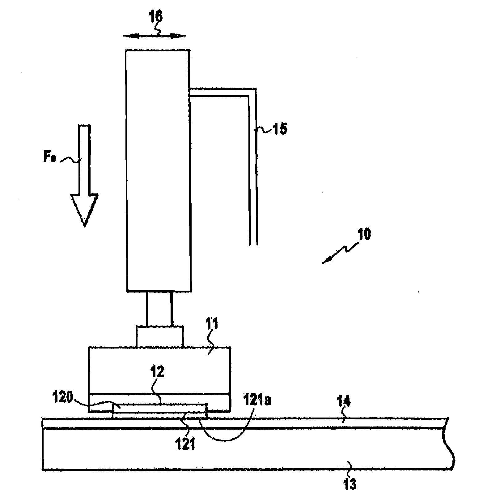
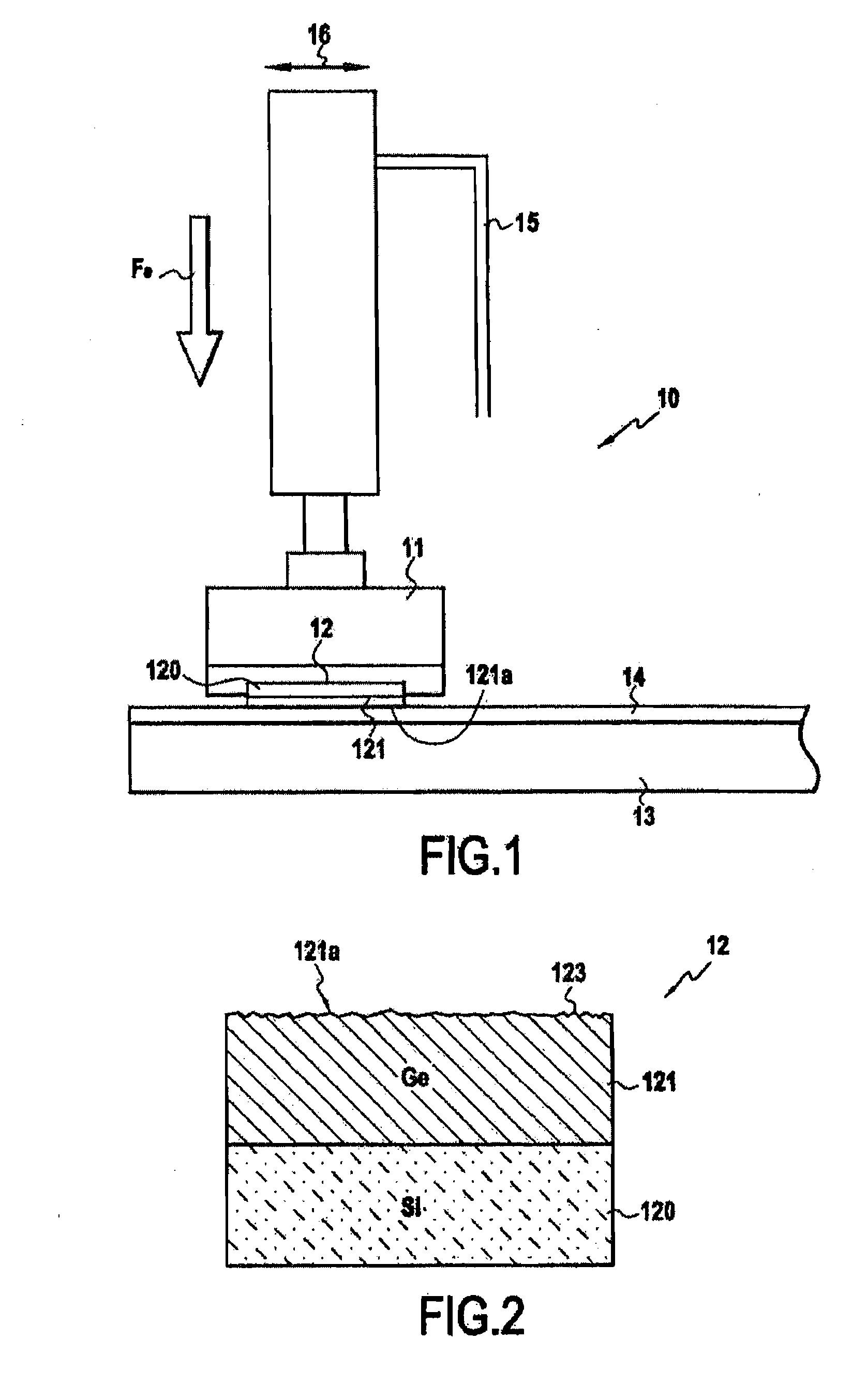
[0032]The method for polishing a germanium layer of the present invention comprises two chemical-mechanical polishing steps, also referred to as CMP polishing, which are carried out consecutively but under different operating conditions. In particular, the first polishing step is carried out with a first polishing solution having an acidic pH, whereas the second polishing step is carried out with a second polishing solution having an alkaline pH.

[0033]More particularly, the first and second polishing solutions contain at least colloidal silica particles and a compound for suspending these particles. A compound having an acidic pH is chosen for the first polishing solution, whereas a compound having an alkaline pH is chosen for the second polishing solution. By way of example, the abrasive solution 30H50 from “Rohm and Haas Company”, USA, may be used for the first polishing solution, and the abrasive solution Klebosol 1508-35 from “Rohm and Haas Company” may be used for the second po...


PUM

PropertyMeasurementUnit
diameteraaaaaaaaaa
diameteraaaaaaaaaa
diameteraaaaaaaaaa

Abstract

In order to polish a layer of germanium (121), a first step of chemical-mechanical polishing of the surface (121a) of the germanium layer (121) is carried out with a first polishing solution having an acidic pH. The first polishing step is followed by a second step of chemical-mechanical polishing of the surface of the germanium layer (121) carried out with a second polishing solution having an alkaline pH.

Description

TECHNICAL FIELD AND PRIOR ART[0001]The present invention relates to the polishing of germanium layers. Germanium is a material which is relatively difficult to polish, whether it is in bulk form (Ge bulk) or obtained by heteroepitaxy on a substrate, for example made of silicon.[0002]In the latter case, when the germanium layer is produced by heteroepitaxy, the crystal lattice mismatch, also referred to as the lattice parameter difference, between the silicon substrate and the epitaxially grown layer of germanium leads to the formation of a dislocated zone (misfit dislocations) at the interface between the silicon substrate and the germanium layer, which leads to the appearance of defects on the surface of the germanium layer, for example a strain network referred to as “cross-hatch”. These defects increase the surface roughness of the epitaxially grown germanium layer.[0003]The surface of the germanium layer should therefore be polished in order to eliminate the potential defects re...

Claims


Application Information

Patent Timeline
Patent Type & Authority Applications(United States)
IPC IPC(8): H01L21/762H01L21/304B24B37/04
CPCB24B37/044H01L21/30625C09G1/02
Inventor MARTINEZ, MURIELBEY, PIERRE
Owner SOITEC SA
Why Eureka
Try Eureka