Delay analysis processing of semiconductor integrated circuit

a technology of integrated circuits and delay analysis, which is applied in the direction of electric digital data processing, instruments, computing, etc., can solve the problems of large clock skew, difficult to completely process lsi chips at once, and difficult to adopt high-precision clock skew in macro delay analysis, so as to achieve optimal lsi design and prevent excessive design margins

Inactive Publication Date: 2011-02-24
NEC CORP
View PDF6 Cites 8 Cited by
  • Summary
  • Abstract
  • Description
  • Claims
  • Application Information

AI Technical Summary

Benefits of technology

[0034]The present invention has outstanding features and effects owing to a unique configuration in the delay analysis processing. Accordingly, in the macro delay analysis on one of subdivisions of the hierarchical architecture of the LSI circuitry or the regional delay analysis on an arbitrary region isolated from a chip layout, clock paths of a macro or arbitrary region are each annotated by the delay information of clock paths obtained in the chip layout or the top layout handling a macro or arbitrary region as a black box. Thus it is possible to preclude excessive design margins, which cannot be precluded in the conventional macro delay analysis or the conventional regional delay analysis, thus achieving the optimum LSI design.

Problems solved by technology

Due to the rapid increase in the sizes of LSI chips, a high machine performance and a large memory capacity are needed to handle EDA (Electronic Design Automation) tools; hence, it becomes difficult to entirely process LSI chips at once.
This clock distribution method suffers from a larger clock skew due to a large number of stages needed to establish synchronization on each chip entirely.
In the macro process performed on a macro having fragmentary clock paths, it is difficult to adopt a high-precision clock skew in the macro delay analysis due to differences of clock paths having different numbers of stages included in clock trees, each of which leads from a clock source (PLL) of an LSI chip to clock terminals at a macro boundary.
A similar drawback occurs when delay analysis is performed on an arbitrary region of the hierarchical architecture of the circuitry subsequently to a chip layout.

Method used


Image

  • Delay analysis processing of semiconductor integrated circuit
  • Delay analysis processing of semiconductor integrated circuit
  • Delay analysis processing of semiconductor integrated circuit

Examples


first embodiment

1. First Embodiment

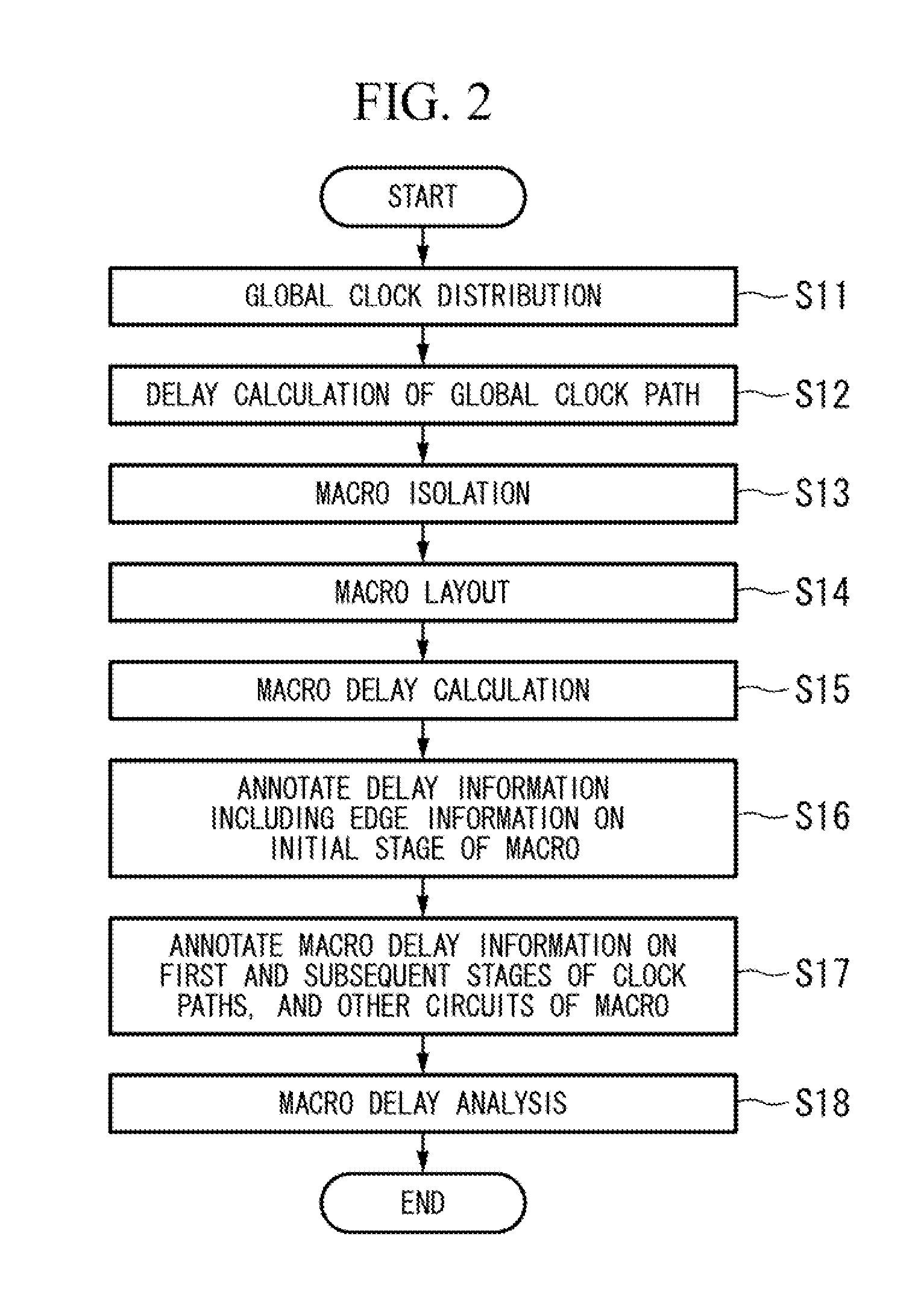
[0049]A delay analysis device for analyzing a semiconductor integrated circuit according to a first embodiment of the present invention will be described with reference to the accompanying drawings. The first embodiment refers to a clock distribution method of “H-Tree”; but this is not a restriction.

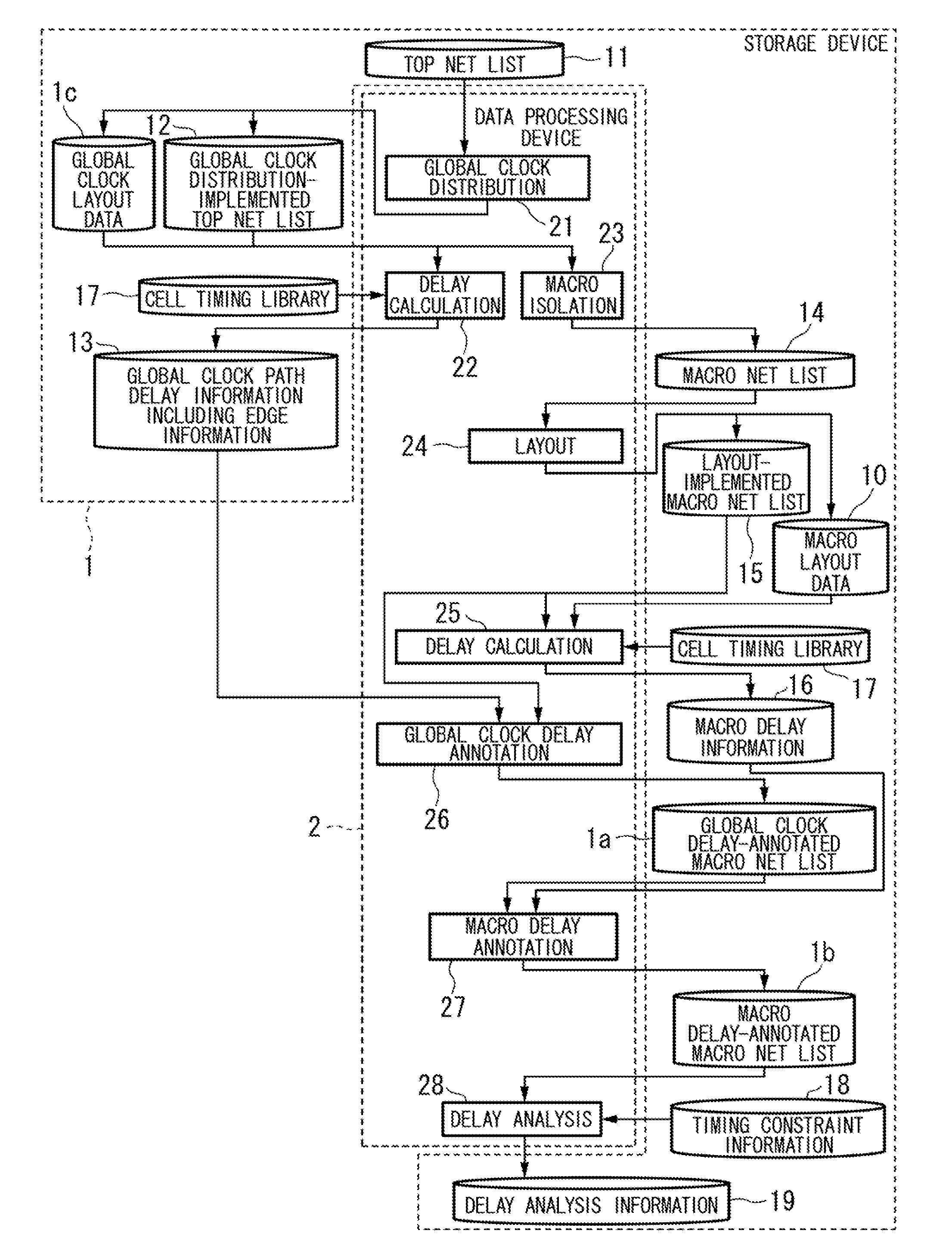
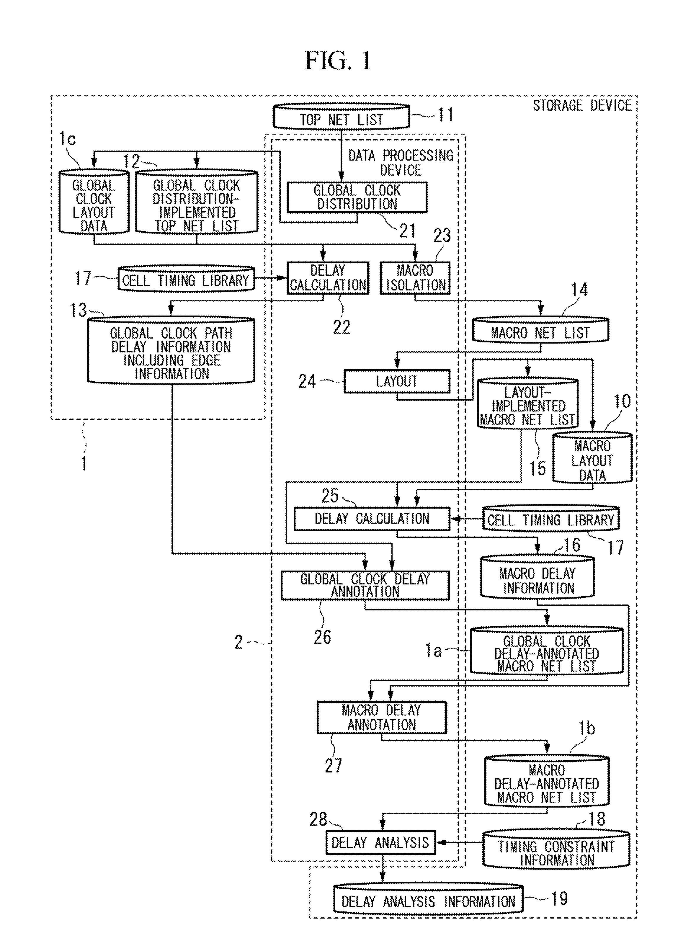
[0050]FIG. 1 is a block diagram of the delay analysis device of the first embodiment, which is constituted of a storage device 1 (e.g. a hard-disk unit) and a data processing device 2 which operates in accordance with programs.

[0051]The storage device 1 stores various files representing a top net list 11, a cell timing library 17, and timing constraint information 18. In addition, the storage device 1 stores various files of output information such as a global clock distribution-implemented top net list 12, a global clock layout data 1c, a global clock path delay information 13 including edge information, a macro net list 14, a layout-implemented macro net list 15, a m...

second embodiment

2. Second Embodiment

[0091]Next, a delay analysis device according to a second embodiment of the present invention will be described in detail. FIG. 8 is a block diagram of the delay analysis device of the second embodiment, wherein parts identical to those shown in FIG. 1 are designated by the same reference numerals.

[0092]The delay analysis device of FIG. 8 is constituted of the storage device 1 (composed of a hard-disk unit or the like) and the data processing device 2 which operates in accordance with programs.

[0093]The storage device 1 stores files representing a chip net list 1d and an external clock path delay information 13 (in which the term “external” is meant to be outside an arbitrary region) including the edge information as well as the cell timing library 17 and the timing constraint information 18. The storage device 1 stores files representing the output information such as a regional net list 1e, a layout-implemented regional net list 1f, regional layout data 1g, reg...


PUM


Abstract

A delay analysis device composed of a storage device and a data processing device analyzes a chip fabricating a semiconductor integrated circuit. Delay calculation is performed via an RC simulation with reference to a layout-implemented macro net list, macro layout data, and a cell timing library, thus producing macro delay information. An initial stage of a macro is annotated by the global clock path delay information including the edge information so as to produce a global clock delay-annotated macro net list, which is then converted into a macro delay-annotated net list. Based on the macro delay-annotated net list and timing constraint, the delay analysis device calculates delay times of signal paths and clock paths as well as clock skews with a high precision. It checks whether or not the relationship between the delay times of signal paths and clock paths meets the timing constraint, thus producing delay analysis information.

Description

[0001]The present application claims priority on Japanese Patent Application No. 2009-191845, the content of which is incorporated herein by reference.BACKGROUND OF THE INVENTION[0002]1. Field of the Invention[0003]The present invention relates to delay analysis processing of semiconductor integrated circuits, and in particular to delay analysis devices, delay analysis methods, and delay analysis programs, all of which perform delay analysis processing on semiconductor integrated circuits subsequently to chip layouts so as to reduce clock skews.[0004]2. Description of the Related Art[0005]Due to the rapid increase in the sizes of LSI chips, a high machine performance and a large memory capacity are needed to handle EDA (Electronic Design Automation) tools; hence, it becomes difficult to entirely process LSI chips at once. To cope with the rapid increase in the sizes of LSI chips, a dominant manufacturing method has been developed to design a single LSI chip in units of hierarchical ...

Claims


Application Information

Patent Timeline
Patent Type & Authority Applications(United States)
IPC IPC(8): G06F17/50
CPCG06F17/5031G06F2217/84G06F2217/62G06F30/3312G06F30/396G06F2119/12
Inventor KANNO, KOJI
Owner NEC CORP
Why Eureka
Try Eureka