Functional device and method for producing the same
a functional device and technology of a functional device, applied in the direction of sustainable manufacturing/processing, instruments, cell components, etc., to achieve the effects of improving durability, reducing conductive catalysts, and improving durability
- Summary
- Abstract
- Description
- Claims
- Application Information
AI Technical Summary
Benefits of technology
Problems solved by technology
Method used
Image

Examples
example 1
Embodiment
Structural Example of Dye-Sensitized Solar Cell (First)
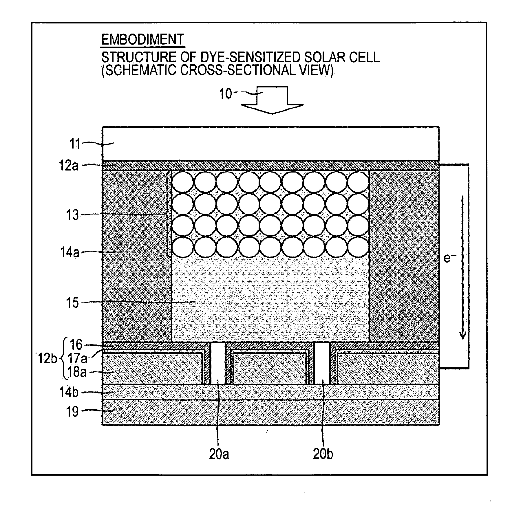
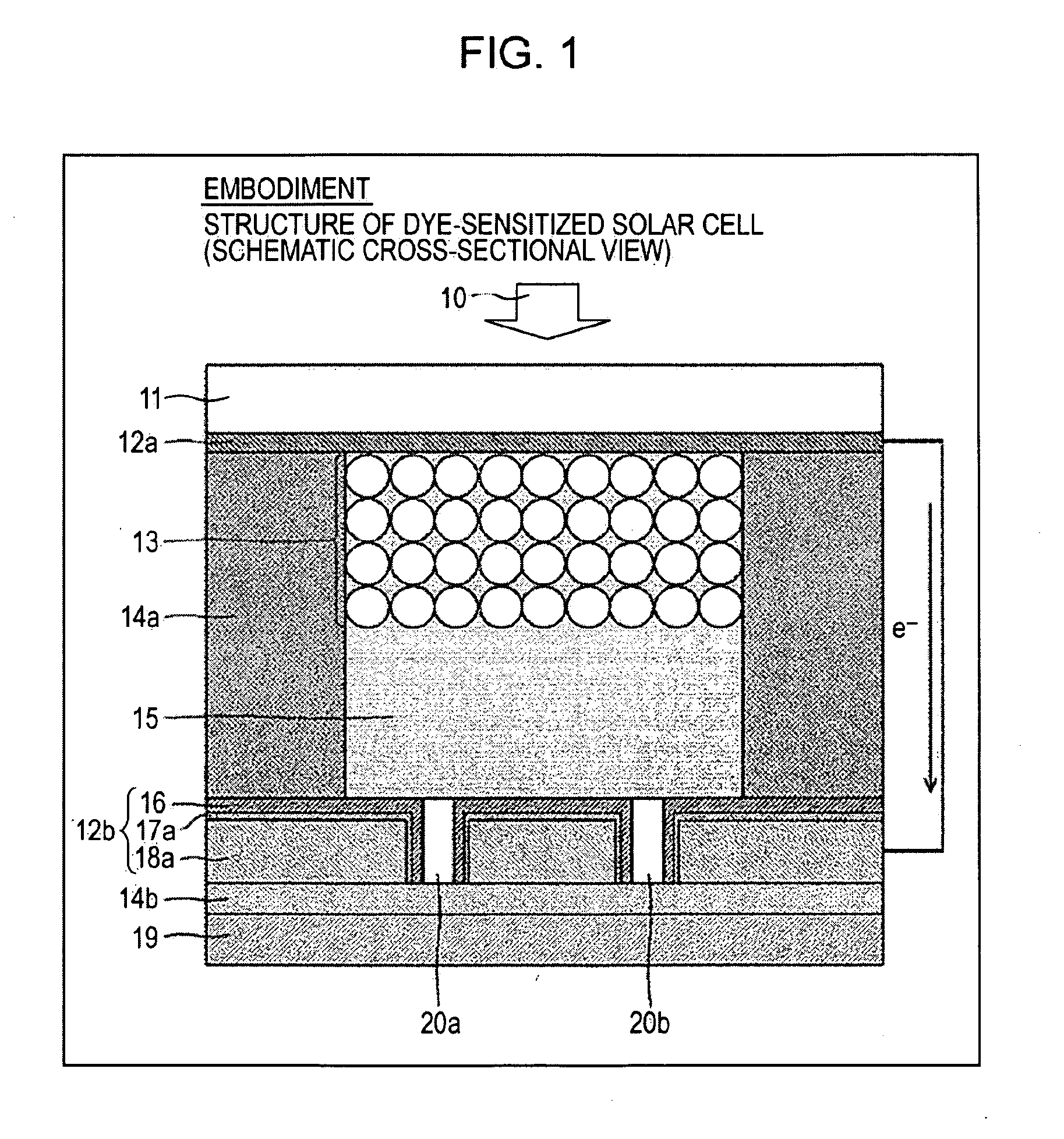
[0061]FIG. 1 is a cross-sectional view schematically showing a structural example of a dye-sensitized solar cell according to an embodiment of the present invention.
[0062]As shown in FIG. 1, the dye-sensitized solar cell includes a photoelectrode on which sunlight 10 is incident, a counter electrode opposed to the photoelectrode, and an electrolyte solution 15 held between the between the two electrodes. The photoelectrode includes a transparent photoelectrode layer (electrode layer, first electrode layer) 12a disposed on a transparent photoelectrode substrate (first substrate) 11, and a semiconductor porous layer 13 carrying a sensitizing dye is disposed on the photoelectrode layer 12a.
[0063]The semiconductor porous layer 13 is, for example, composed of nanosized titanium oxide (TiO2), and the sensitizing dye is, for example, a ruthenium bipyridyl complex. The counter electrode is constituted by a counter electrode s...
example
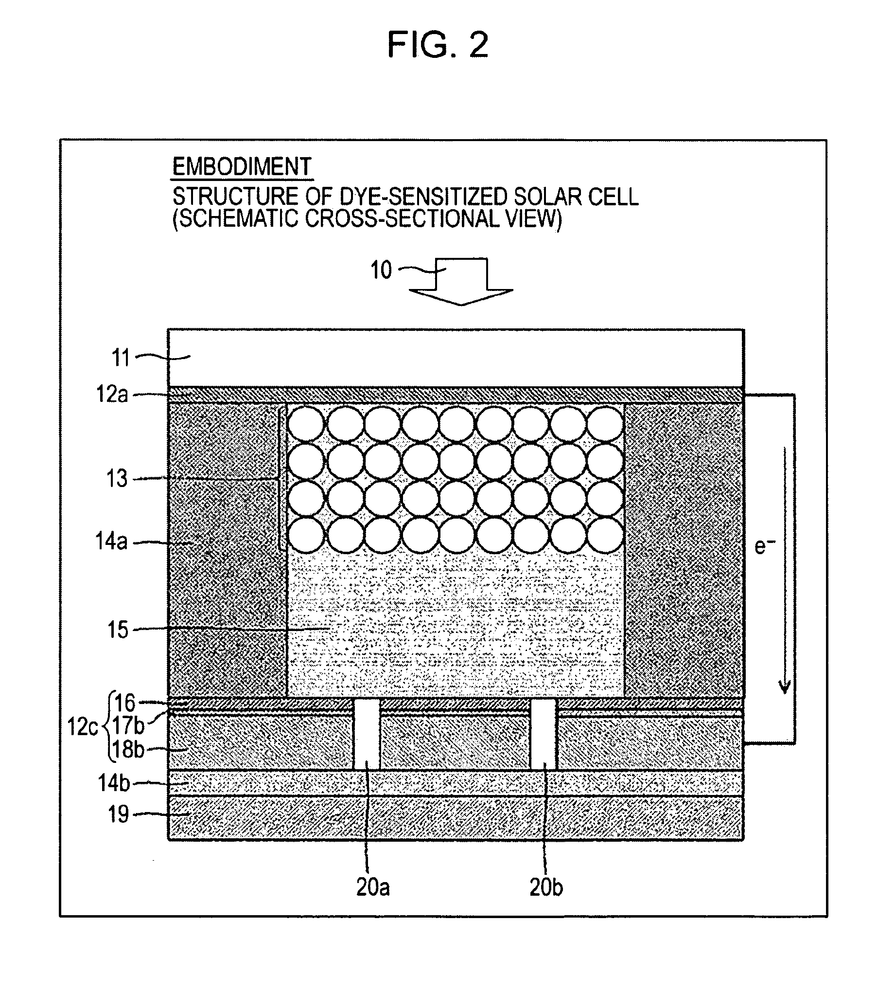
[0183]The dye-sensitized solar cell in Example of the present invention has the structure shown in FIG. 2.
[0184][Photoelectrode]
[0185]A glass substrate (15 mm×20 mm rectangular, sheet resistance 10 Ω / square, manufactured by Nippon Sheet Glass Co., Ltd.) having a fluorine-doped tin oxide conductive layer (FTO layer) provided thereon as a photoelectrode layer 12a was used as a photoelectrode.
[0186][Semiconductor Porous Layer]
[0187]A semiconductor porous layer 13 was formed on the FTO layer. The semiconductor porous layer 13 was formed by applying titanium oxide (TiO2) with a medium particle diameter of 20 nmφ at a thickness of 15 μm as a lower layer and titanium oxide (TiO2) with a medium particle diameter of 400 nmφ at a thickness of 5 μm as an upper layer with a screen printing machine, and then performing sintering treatment at 510° C. for 30 minutes.
[0188][Sensitizing Dye and Carrying Thereof]
[0189]FIG. 8 is a diagram showing examples of the sensitizing dye used in Example of the ...
PUM
| Property | Measurement | Unit |
|---|---|---|
| thickness | aaaaa | aaaaa |
| thickness | aaaaa | aaaaa |
| thickness | aaaaa | aaaaa |
Abstract
Description
Claims
Application Information
 - Generate Ideas
- Intellectual Property
- Life Sciences
- Materials
- Tech Scout
- Unparalleled Data Quality
- Higher Quality Content
- 60% Fewer Hallucinations
Browse by: Latest US Patents, China's latest patents, Technical Efficacy Thesaurus, Application Domain, Technology Topic, Popular Technical Reports.
© 2025 PatSnap. All rights reserved.Legal|Privacy policy|Modern Slavery Act Transparency Statement|Sitemap|About US| Contact US: help@patsnap.com