Recessed contact for multi-gate FET optimizing series resistance

a contact and series resistance technology, applied in the field of field effect transistors, can solve the problems of significant deformation of drive current, and achieve the effect of reducing parasitic resistan

Active Publication Date: 2011-03-03
AURIGA INNOVATIONS INC
View PDF13 Cites 47 Cited by
  • Summary
  • Abstract
  • Description
  • Claims
  • Application Information

AI Technical Summary

Benefits of technology

[0006]What is needed is a technique to reduce the parasitic

Problems solved by technology

Semiconductors and integrated circuit chips have become ubiquitous within many products due to their continually decreasing cost and size.
However, such small dimensions necessitate greater control over performance issues such as short channel effects, punch-through, metal-oxide semicondu

Method used


Image

  • Recessed contact for multi-gate FET optimizing series resistance
  • Recessed contact for multi-gate FET optimizing series resistance
  • Recessed contact for multi-gate FET optimizing series resistance

Examples


Embodiment Construction

[0016]It is noted that one possible approach to reduce the parasitic resistance can be to use highly angled implants to the extension region in conjunction with the selective epitaxial regrowth of the S / D region. However, the simultaneous vertical epitaxial re-growth of the S / D regions limits the improvement of the series resistance.

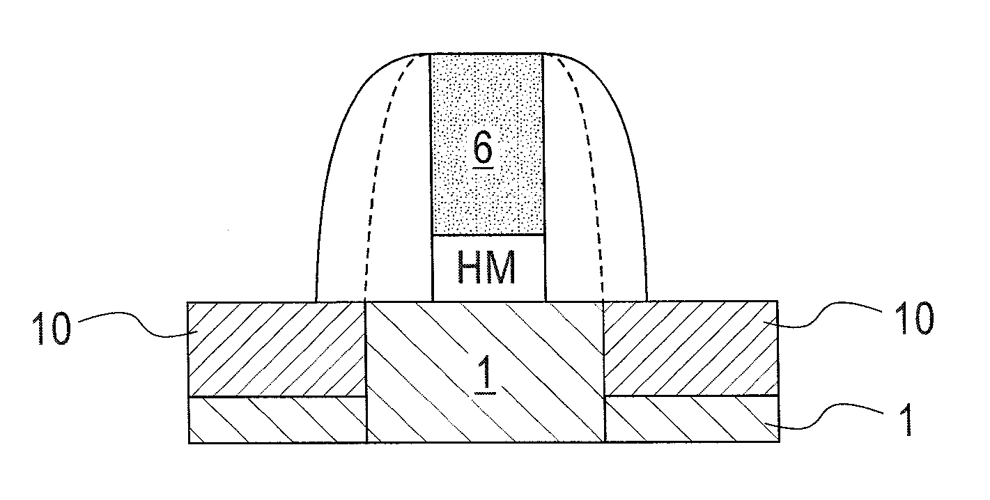
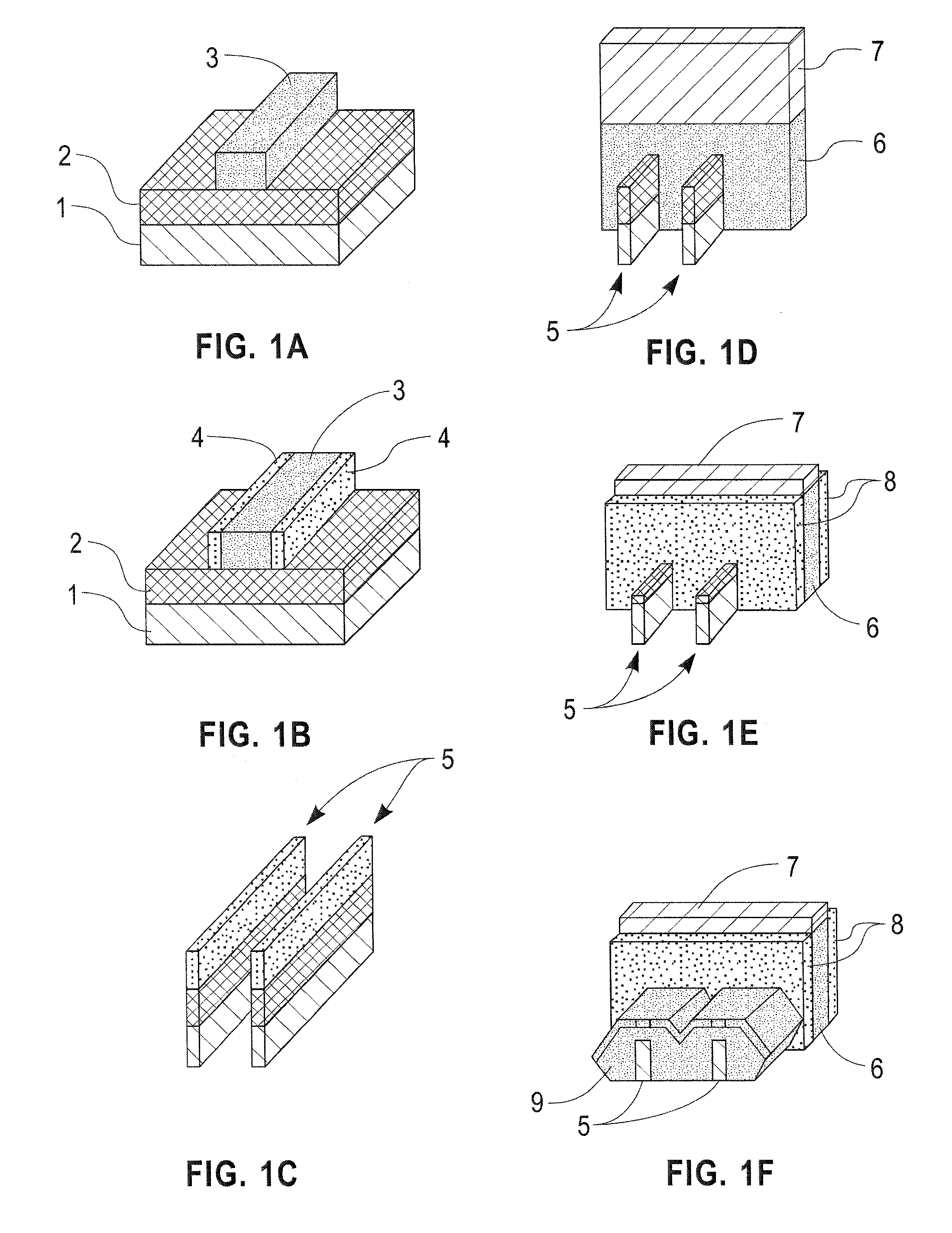
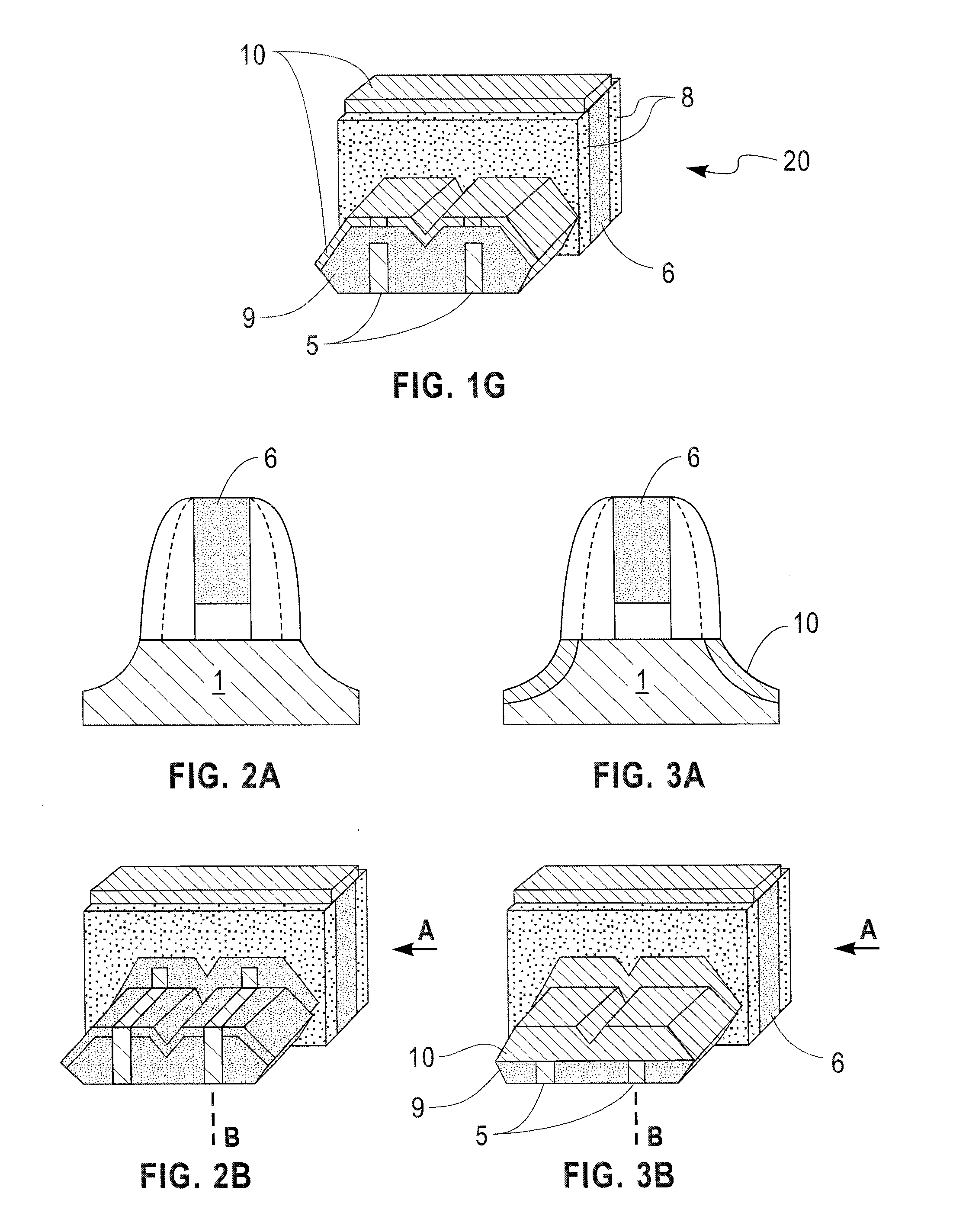
[0017]The exemplary embodiments of this invention are described below in the context of a FinFET. FIGS. 1A-1G provide an overview of one exemplary technique to fabricate a FinFET. FIGS. 2A, 2B, 3A and 3B illustrate a technique to modify the fabrication procedure to provide a FinFET having a reduced parasitic contact resistance in accordance with the exemplary embodiments of this invention.

[0018]FIGS. 1A-1G are presented in the context of side wall image transfer (SIT) fabrication technique that uses a spacer as a hard mask to define the fin. However, this is but one suitable FinFET fabrication technique, and should not be construed in a limiting sense up...


PUM


Abstract

A transistor, which can be referred to as a multi-gate transistor or as a FinFET, includes a gate structure having a length, a width and a height. The transistor further includes at least one electrically conductive channel or fin between a source region and a drain region that passes through the width of the gate structure. The channel has a first height (h1) within the gate structure that is less than the height of the gate structure, and has a second height (h2) external to the gate structure, where h2 is less than h1. The transistor further includes a silicide layer disposed at least partially over the at least one channel external to the gate structure. Reducing the fin height external to the gate structure is shown to beneficially reduce parasitic resistance.

Description

TECHNICAL FIELD[0001]The exemplary embodiments of this invention relate generally to field effect transistors (FETs) and, more specifically, relate to FET contact structures.BACKGROUND[0002]Semiconductors and integrated circuit chips have become ubiquitous within many products due to their continually decreasing cost and size. Miniaturization in general allows increased performance (more processing per clock cycle and less heat generated) at lower power levels and lower cost. Present technology is at or approaching atomic level scaling of certain micro-devices such as logic gates, FETs, capacitors, etc. Circuit chips with hundreds of millions of such devices are not uncommon. Further size reductions appear to be approaching the physical limit of trace lines and micro-devices that are embedded upon and within their semiconductor substrates. The present invention is directed to such micro-sized FET devices.[0003]Basically a FET is a transistor having a source, a gate, and a drain. The...

Claims


Application Information

Patent Timeline
IPC IPC(8): H01L29/78H01L21/336
CPCH01L29/66636H01L29/785H01L29/66795
Inventor LIN, CHUNG-HSUNCHANG, JOSEPHINE B.
Owner AURIGA INNOVATIONS INC
Why Eureka
Try Eureka