
Eureka
For R&D, Eureka makes reading and utilizing patents & technical documents easy.
Eureka AIR
Designed for self-driven R&D workflows. Generate viable solutions, solve complex R&D challenges, empower your innovation with AI.

Eureka Materials
Designed for material experts only. Revolutionize your material R&D, from search, analyze, to developing new materials.

TechResearch
Generate reliable direction feasibility study reports for your R&D in just a few steps.

TechSeek
Discover and master advanced knowledge NOW. Basics, ideas, possibilities, all at once.

TechMind
As an expert in R&D Theories, TechMind can generates customized viable solutions instantly.

TechRisk
Analyze your overall solution with one click, know your potential R&D risks in advance.

TechMonitor
Get weekly tech updates, stay abreast of the latest tech innovations and key insights.
Da converter and solid-state imaging device
- Summary
- Abstract
- Description
- Claims
- Application Information
AI Technical Summary
Benefits of technology
Problems solved by technology
Method used
Image

Examples
first embodiment
1. First Embodiment
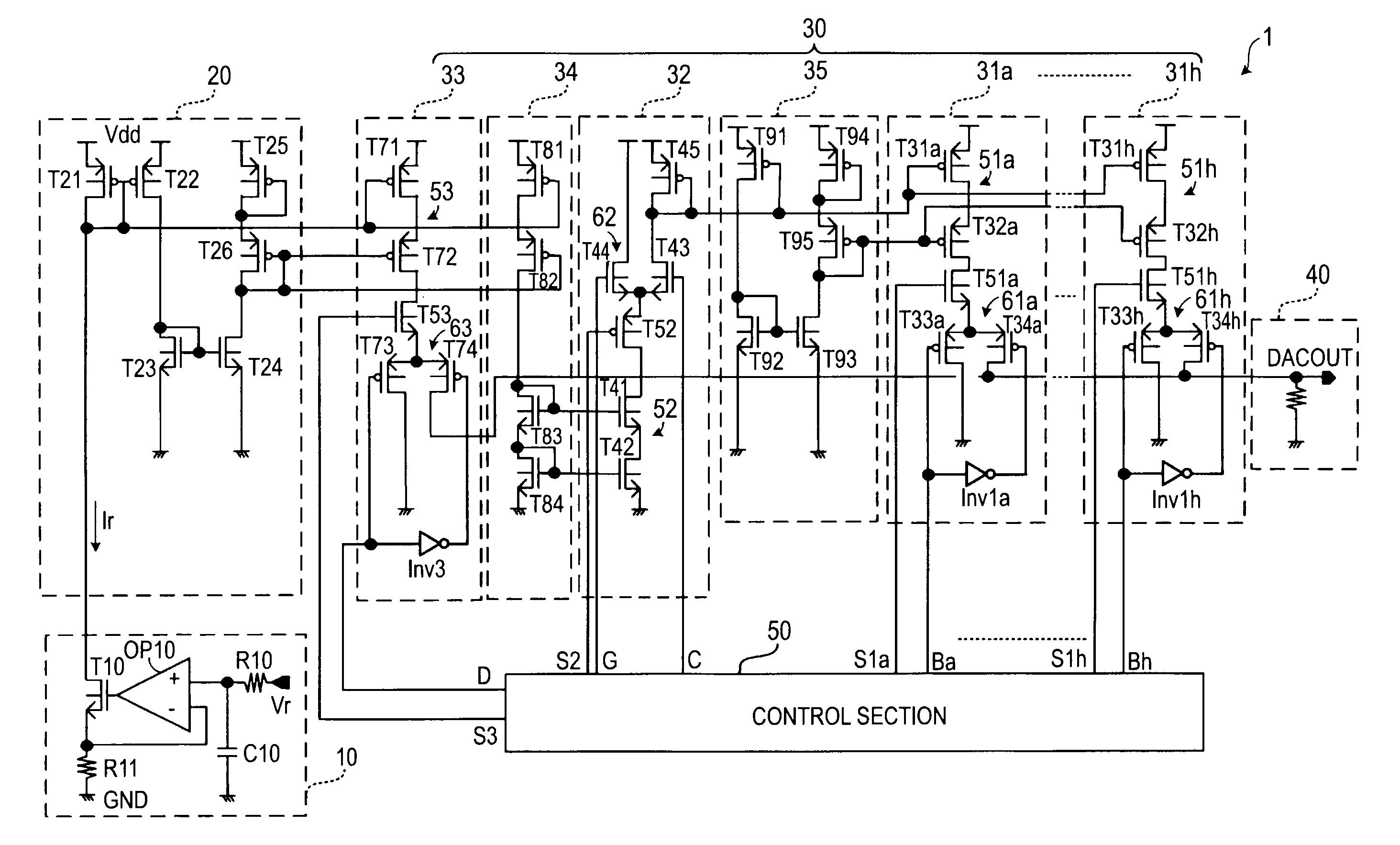
[0050]First, a DA converter according to the first embodiment will be described specifically referring to FIG. 1.
(General Configuration of DA Converter)
[0051]As shown in FIG. 1, a DA converter 1 according to the first embodiment has a reference current generating circuit 10, a current transfer circuit part 20, a current source section 30, a voltage output circuit 40, and a control section 50.
[0052]The reference current generating circuit 10 generates a reference current Ir according to an input reference voltage Vr. A current corresponding to the reference current Ir generated by the reference current generating circuit 10 is transferred to the current source section 30 via the current transfer circuit part 20. The current source section 30 has a plurality of current sources from which one current source to be connected to the voltage output circuit 40 is selected by the control section 50. The voltage output circuit 40 includes a resistor R across which the curre...
second embodiment
2. Second Embodiment
[0092]Next, a solid-state imaging device according to the second embodiment will be described specifically referring to FIG. 6. This solid-state imaging device is a CMOS image sensor to which the DA converter according to the first embodiment is adapted.
[0093]As shown in FIG. 6, a solid-state imaging device 100 has a pixel array section 101 as an imaging section, a row scan circuit 102, a column scan circuit 103, a control circuit 104, an ADC group 105, a DA converter 106, a horizontal output line 107, and an output amplifier 108. The DA converter 106 has the same configuration as the DA converter according to the first embodiment.
[0094]The pixel array section 101 has a two-dimensional array of unit pixels 110 each of which converts the amount of the input light to an electric signal. The unit pixel 110 is provided with a photodiode to perform photoelectric conversion, a transfer transistor to read a signal charge generated by the photodiode, and an amplification...
PUM
 Abstract
Description
Claims
Application Information
 - R&D Engineer
- R&D Manager
- IP Professional
- Industry Leading Data Capabilities
- Powerful AI technology
- Patent DNA Extraction
Browse by: Latest US Patents, China's latest patents, Technical Efficacy Thesaurus, Application Domain, Technology Topic, Popular Technical Reports.
© 2024 PatSnap. All rights reserved.Legal|Privacy policy|Modern Slavery Act Transparency Statement|Sitemap|About US| Contact US: help@patsnap.com