Image sensor structure and fabricating method therefor

a technology of image sensor and manufacturing method, which is applied in the direction of electrical equipment, semiconductor devices, radio frequency controlled devices, etc., can solve the problems of reducing the focal length, and reducing the focal angl

Active Publication Date: 2011-03-10
UNITED MICROELECTRONICS CORP
View PDF5 Cites 39 Cited by
  • Summary
  • Abstract
  • Description
  • Claims
  • Application Information

AI Technical Summary

Benefits of technology

[0012]In the image sensor structure according to the present invention, an under layer is disposed beneath a filter array. The under layer is filled into the dishing-shaped top surface structure of the underlying dielectric layer. Material for the under layer is selected, such that the under layer can play as a role of a convex lens to compensate the focal length difference between the center and the edge of the sensor array, in addition to functions of adhesion and planarization. Hence, the photo-response in one chip will be more uniform.

Problems solved by technology

For digital imaging apparatuses, such as digital still cameras or digital video cameras, image quality is one of the most significant design issues.
However, with the demand for lighter, thinner, shorter, and smaller devices, the focal length must be shortened.
However, as shorter focal length is demanded, the chief-ray angle becomes greater, where the shifting of the microlenses or the color filters is spatially limited and can not well compensate the shading effect.

Method used


Image

  • Image sensor structure and fabricating method therefor
  • Image sensor structure and fabricating method therefor
  • Image sensor structure and fabricating method therefor

Examples


Embodiment Construction

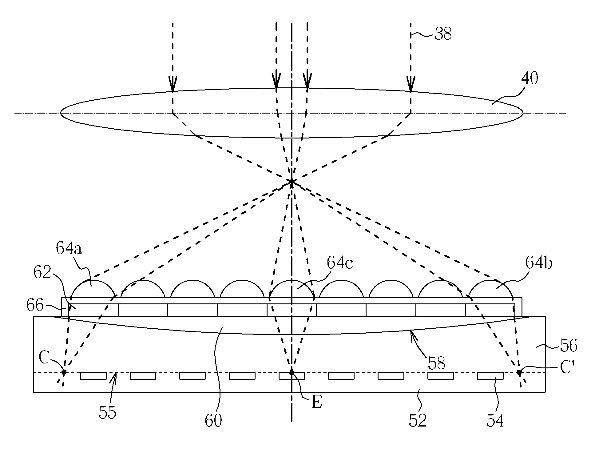
[0021]The image sensor structure according to the present invention may be applied to CMOS image sensor (CIS) devices or charge coupled devices (CCD) FIG. 4 illustrates a cross-sectional diagram of an embodiment of the image sensor structure according to the present invention. As shown in FIG. 4, the image sensor structure 50 includes a substrate 52, a sensor array 54, a dielectric layer 56, an under layer 60, a filter array 62, and a microlens array 64. The substrate 52 may be for example a semiconductor substrate. The sensor array 54, i.e. an array of sensing elements, is disposed at the surface of the substrate 52. It may be disposed in or on the substrate surface without particular limitation but in accordance with the properties of the sensing element or device design. The sensing element may be, for example, photo-sensing element, such as photodiode. The dielectric layer 56 covers the sensor array 54 and the substrate 52. The dielectric layer 56 includes a top surface 58 and i...


PUM


Abstract

An image sensor structure and a method for making the image sensor structure, for avoiding or mitigating lens shading effect. The image sensor structure includes a substrate, a sensor array disposed at the surface of the substrate, a dielectric layer covering the sensor array, wherein the dielectric layer includes a top surface having a dishing structure, an under layer filled into the dishing structure and having a refraction index greater than that of the dielectric layer, a filter array disposed on the under layer corresponding to the sensor array, and a microlens array disposed above the filter array. A top layer may be additionally disposed to cover the filter array and the microlens array is disposed on the top layer.

Description

BACKGROUND OF THE INVENTION[0001]1. Field of the Invention[0002]The present invention relates to an image sensor structure and a method of fabricating the same, and particularly to an image sensor structure and a method of fabricating the same capable of avoiding or mitigating shade effect.[0003]2. Description of the Prior Art[0004]For digital imaging apparatuses, such as digital still cameras or digital video cameras, image quality is one of the most significant design issues. In an image generated by an image sensor of a conventional digital imaging apparatus, the central portion of the image is typically brighter than the peripheral portion of the image. This phenomenon is also referred to as lens shading effect or vignetting phenomenon, which is caused by a non-uniform photo-response across the lens of the digital imaging apparatus. It is found that if the chief ray angle is greater than 20 degrees, the brightness of the peripheral image is 78% or less of the brightness of the c...

Claims


Application Information

Patent Timeline
Patent Type & Authority Applications(United States)
IPC IPC(8): H01L31/0232H01L31/18H01L31/0216
CPCH01L27/14621H01L27/14629H01L27/14627H01L27/14623
Inventor YU, CHENG-HUNG
Owner UNITED MICROELECTRONICS CORP
Why Eureka
Try Eureka