

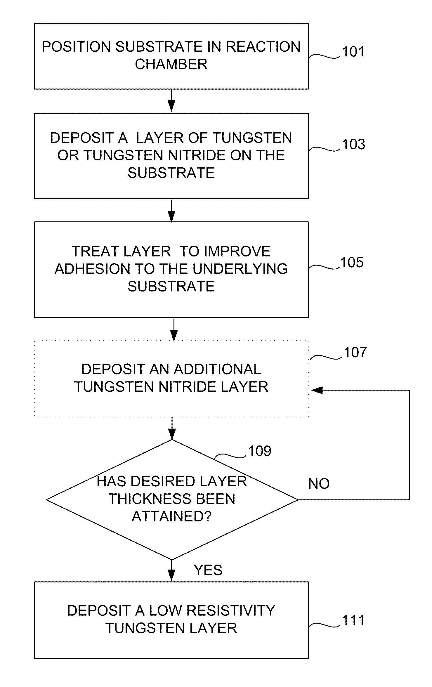
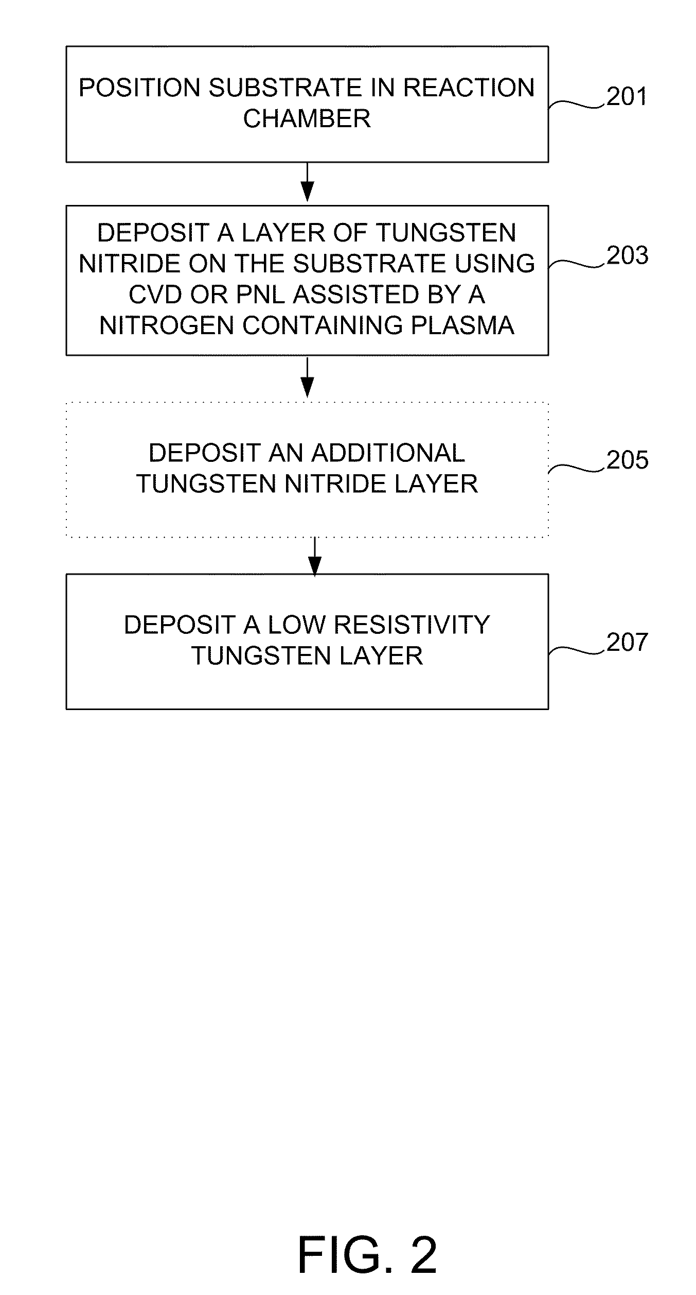
Method for improving adhesion of low resistivity tungsten/tungsten nitride layers
a technology of tungsten nitride and low resistivity, which is applied in the direction of coating, chemical vapor deposition coating, plasma technique, etc., can solve the problems of preventing these materials from being used together in semiconductor devices, and achieve good adhesion to the underlying layer, improve adhesion to the underlying substrate, and reduce the effect of resistan
- Summary
- Abstract
- Description
- Claims
- Application Information
AI Technical Summary
Problems solved by technology
Method used
Image

Examples
example 1
Plasma Treatment
[0050]A 30 Angstrom thick tungsten nitride layer was first deposited on a silicon oxide under layer using a PNL process. The substrate was kept and 325° C. during this process, and tungsten hexafluoride, diborane, and ammonia were used in the PNL process. A hydrogen plasma at 10 mTorr was used for the plasma treatment. After treatment, a tungsten nucleation layer was first deposited onto the tungsten nitride layer using a PNL process and then treated to lower its resistivity. Two different low resistivity tungsten / tungsten nitride layers, A and B, were formed using different low-resistivity treatments for the tungsten nucleation layer in this example. Tungsten nucleation layer treatment A comprised holding the substrate at a temperature of 300° C. and exposing the tungsten nucleation layer to alternating pulses of diborane and tungsten hexafluoride. Tungsten nucleation layer treatment B comprised holding the substrate at a temperature of 395° C. and exposing the tung...
example 2
No Adhesion Treatment
[0053]A 55 Angstrom thick tungsten nitride layer was first deposited on a silicon oxide under layer using a PNL process. The substrate was kept and 325° C. during this process, and tungsten hexafluoride, diborane, and ammonia were used in the PNL process. The tungsten nitride layer was not treated prior to the deposition of the low resistivity tungsten layer. A tungsten nucleation layer was first deposited onto the tungsten nitride layer using a PNL process, and then treated to lower its resistivity. The tungsten nucleation layer treatment comprised holding the substrate at a temperature of 300° C. and exposing the tungsten nucleation layer to alternating pulses of diborane and tungsten hexafluoride. Then, a tungsten bulk layer deposited using CVD, resulting in a tungsten layer 1500 Angstroms thick. The process conditions used in this example are also shown in Table II.
TABLE IIProcess conditions used to depositlow resistivity tungsten / tungsten nitride in example...
PUM
| Property | Measurement | Unit |
|---|---|---|
| thickness | aaaaa | aaaaa |
| thick | aaaaa | aaaaa |
| temperature | aaaaa | aaaaa |
Abstract
Description
Claims
Application Information