Semiconductor chip stacked structure and method of manufacturing same

Inactive Publication Date: 2011-03-17
SHINKO ELECTRIC IND CO LTD
View PDF3 Cites 22 Cited by
  • Summary
  • Abstract
  • Description
  • Claims
  • Application Information

AI Technical Summary

Benefits of technology

[0013]According to at least one embodiment, the product quality of a semi

Problems solved by technology

Due to the complexity of semiconductor package structures and manufacturing methods, however, the chip stack technology has not yet sufficiently satisfied the above-noted demand in the industry for improved performance and further miniaturization.
Due to such staircase-form connections, the lengths of the bonding wires are long, which may result in degradation of electrical characteristics.
Further, the chip stack staircase

Method used


Image

  • Semiconductor chip stacked structure and method of manufacturing same
  • Semiconductor chip stacked structure and method of manufacturing same
  • Semiconductor chip stacked structure and method of manufacturing same

Examples


first embodiment

Variation of First Embodiment

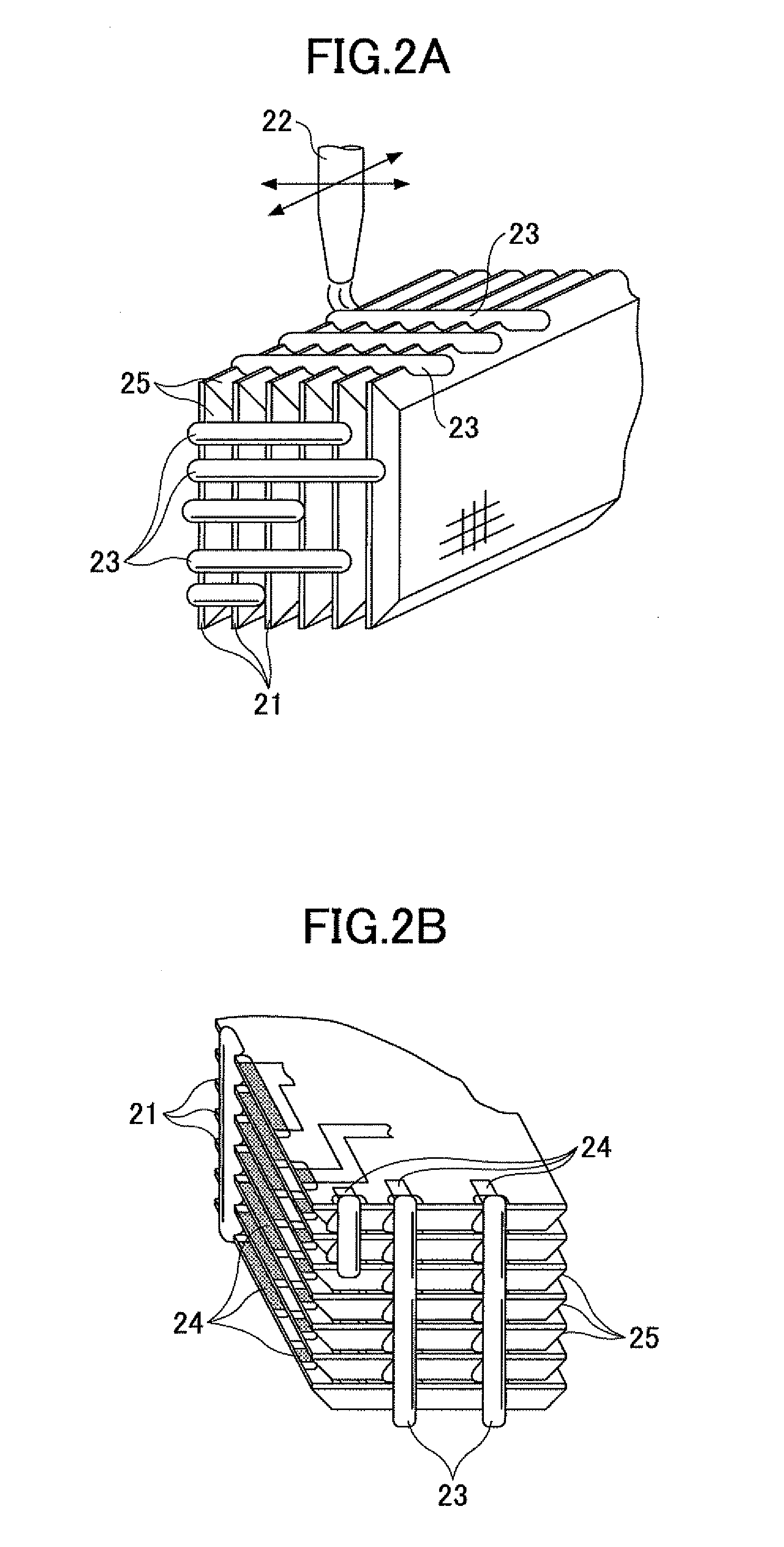
[0082]In the sub-step 2-a of placing semiconductor chips on a tentative adhesive film according to the first embodiment, the semiconductor chips are placed at respective positions on the tentative adhesive film in order to provide sufficient spacing intervals between the semiconductor chips. In a variation thereof, placement for providing spacing intervals is achieved by use of another means. That is, a dicing tape for supporting a semiconductor wafer at the time of dicing is stretched and expanded in the radial directions of the wafer after the dicing, thereby providing sufficient spacing intervals between the semiconductor chips.

[0083]FIG. 6 is a flowchart illustrating a method of manufacturing a semiconductor chip stacked structure according to the variation of the first embodiment.

[0084]The manufacturing method includes a dicing step S601, a chip sealing structure forming step S602, a chip face exposing step S603, an electrical connection providing s...

second embodiment

Advantage of Second Embodiment

[0103]A manufacturing method is provided to mount a chip stacked structure on a wiring substrate in a flip-chip manner. With this method, a small-size chip stacked structure comparable in size to the chips can be mounted on the wiring substrate in a short time. The productivity and quality of semiconductor chip stacked structures can thus be improved. Further, the method of providing flip-chip connection as illustrated in FIG. 10B can expand the range of semiconductor chip types that can be used in the semiconductor chip stacked structure. For example, a CPU serving as a logic circuit having a large number of terminals may be stacked with memory semiconductor chips, thereby contributing to functional expansion.

Third Embodiment

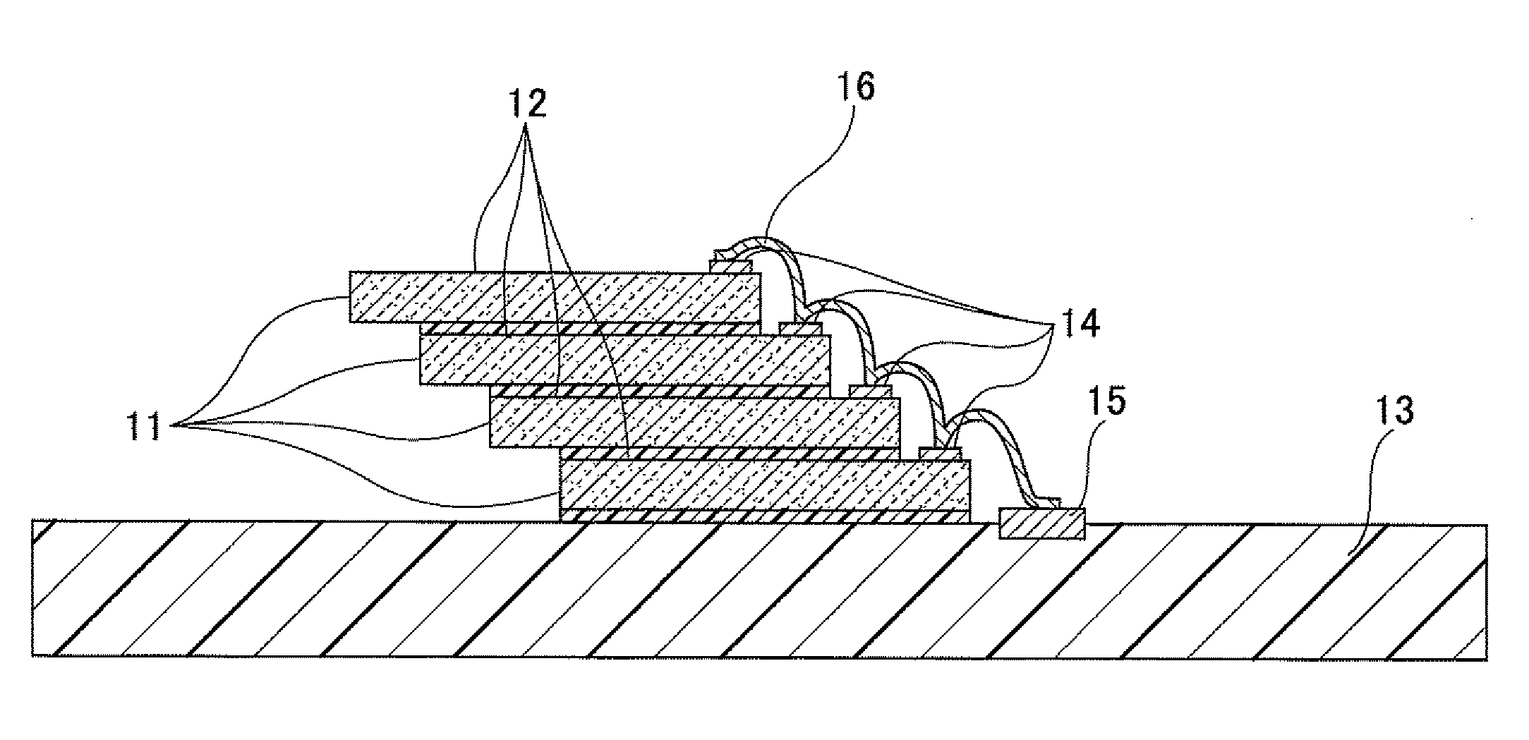
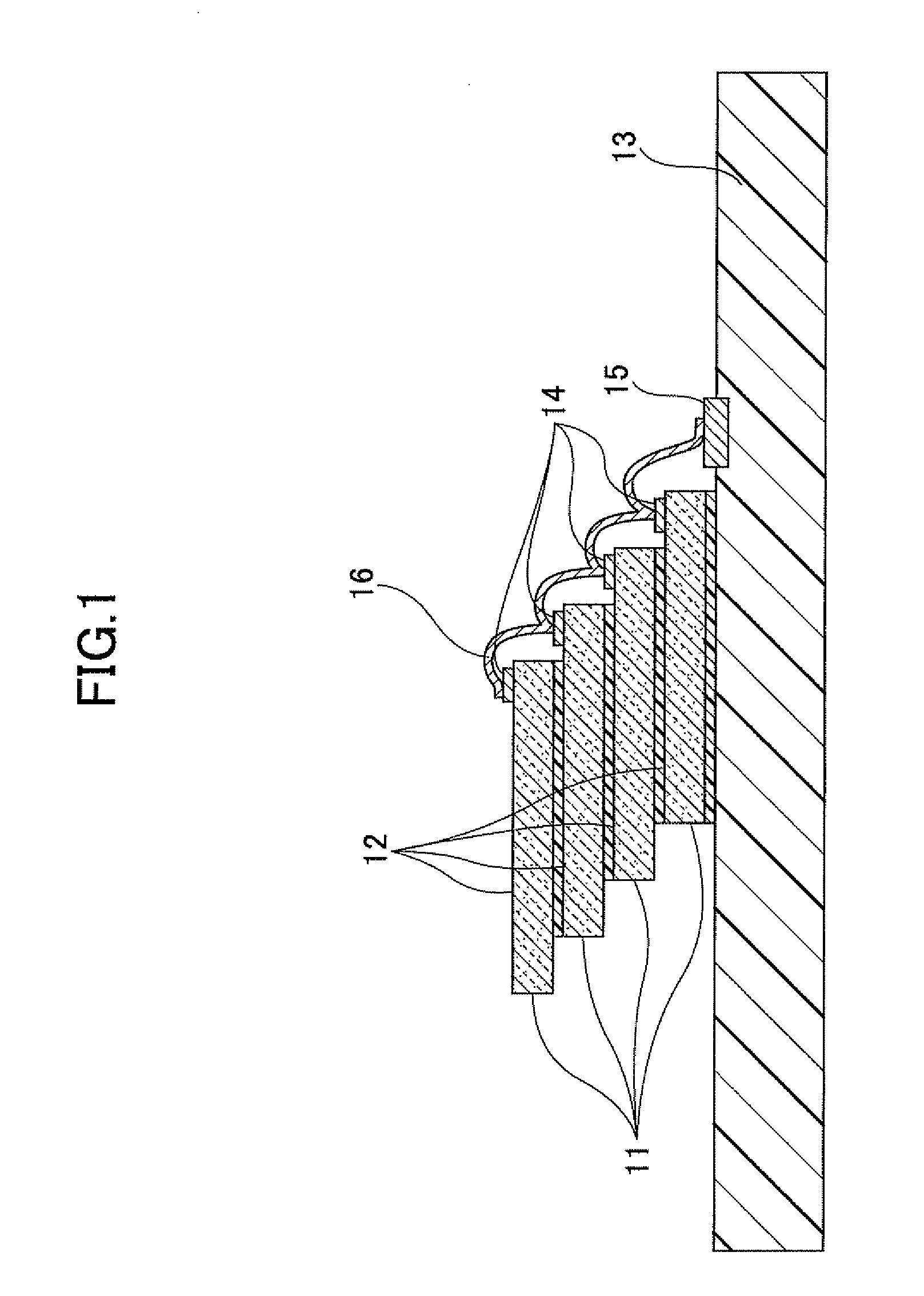
[0104]The third embodiment is directed to a semiconductor chip stacked structure that includes a wiring substrate and a stack of plural chip sealing structures each of which has the back surface of the chip being exposed.

[0105]FIG....

third embodiment

Variation of Third Embodiment

[0109]FIGS. 11A through 11C are drawings illustrating beveled corners of the chip sealing structures according to a variation of the third embodiment. Corners 50C are beveled, so that the angle at which the electrically conductive joining members are cut is set equal to a sharp angle. This serves to broaden the connection faces of the electrically conductive joining members that meet bonding wires. Beveling is performed to provide a flat surface in FIG. 11A, and is performed to provide a curved surface in FIG. 11B. In FIG. 11A, a flat beveled surface is provided at the corners of chip sealing structures 111, thereby forming an angle βsmaller than the right angle between a resin surface 115 and the axial direction P of an electrically conductive joining member 113 at an end face 114 thereof. This arrangement serves to provide a reliable electrical connection as in the case of FIG. 5C, in which the electrically conductive joining member 54 is bent such tha...


PUM


Abstract

A method of making a semiconductor chip stacked structure includes dicing a semiconductor wafer into semiconductor chips, the semiconductor chips respectively having a first surface and a second surface opposite thereto, the semiconductor chips having integrated circuits and pads on the first surfaces, arranging the semiconductor chips at intervals on a film having adhesive property, connecting the pads through joining members, sealing with resin the joining members and surfaces of the semiconductor chips excluding the second surfaces to produce a chip sealing structure, dividing the chip sealing structure to produce separate chip sealing structures having ends of the joining members exposed at surfaces thereof, removing the film to expose the second surfaces, stacking the chip sealing structures one over another and connecting the exposed ends of the joining members through a bonding wire to produce a chip stacked structure, and mounting the chip stacked structure on a wiring substrate.

Description

BACKGROUND OF THE INVENTION[0001]1. Field of the Invention[0002]The disclosures herein relate to a semiconductor chip stacked structure and a method for manufacturing a semiconductor chip stacked structure.[0003]2. Description of the Related Art[0004]A chip size package (i.e., CSP) in which a semiconductor chip is packaged is utilized as a semiconductor device mounting technology that achieves high density. A CSP is a package that is obtained by dividing and processing a semiconductor wafer including integrated circuits. CSPs may be used individually or combined together for use in mobile information devices or small-size electronic devices. The CSP technology is expected to contribute to the improved performance and further miniaturization of such devices. In response to an increase in memory capacity, for example, a chip stacked structure may be used together with the CSP technology.[0005]As disclosed in Patent Document 1 and Patent Document 2, various studies have been made with ...

Claims


Application Information

Patent Timeline
IPC IPC(8): H01L23/522H01L21/50
CPCH01L21/568H01L23/3107H01L24/24H01L24/45H01L24/48H01L24/73H01L25/0657H01L25/50H01L2224/24145H01L2224/32145H01L2224/32225H01L2224/45124H01L2224/45144H01L2224/45184H01L2224/48091H01L2224/48145H01L2224/48147H01L2224/48227H01L2224/48599H01L2224/48699H01L2224/73207H01L2224/73265H01L2224/85099H01L2224/8593H01L2224/85951H01L2225/06506H01L2225/0651H01L2225/06551H01L2225/06562H01L2924/01013H01L2924/01029H01L2924/01047H01L2924/0105H01L2924/01079H01L2924/014H01L2924/01005H01L2924/01006H01L2924/01019H01L2924/01033H01L2924/01074H01L21/561H01L24/16H01L24/81H01L2224/16225H01L2224/81411H01L2224/81439H01L2224/81447H01L2924/1815H01L2924/18161H01L2924/19107H01L2224/45015H01L2224/45147H01L2924/00014H01L2924/00012H01L2924/00H01L2924/2076H01L2224/02371H01L2224/03334H01L2224/0401H01L2224/04105H01L2224/05548H01L2224/45014H01L2224/85203H01L2224/85205H01L2924/14H01L2924/181H01L2224/85399H01L2224/05599H01L2924/206
Inventor MURAYAMA, KEIAIZAWA, MITSUHIRO
Owner SHINKO ELECTRIC IND CO LTD
Why Eureka
Try Eureka