Semiconductor integrated circuit device and system

Active Publication Date: 2011-03-17
RENESAS ELECTRONICS CORP
View PDF18 Cites 33 Cited by
  • Summary
  • Abstract
  • Description
  • Claims
  • Application Information

AI Technical Summary

Benefits of technology

[0017]On the other hand, at the time of power gating, by a control circuit (RSCNT) of the peripheral circuit (peripheral) of the other static type RAMs (SRAM2, SRAM3) coupled to the other local power source vssm22, the peripheral circuit power switches PESW22 and PESW23 are controlled into an off state, and the source line potential control circuit arvss_control sets potential of the cell array source lines arvss22, arvss23 of the cell arrays (cell_array) of the other static type RAMs (SRAM2, SRAM3) to a little higher level than the ground potential Vss. Therefore, due to the off state of the peripheral circuit power switches PESW22, PESW23, it is possible to cut off a leakage current of the peripheral circuits (peripheral) other than a control circuit (RSCNT) and a part of circuits such as a word driver. Furthermore, due to the potential of a little higher level than the ground potential Vss of the cell array source lines arvss22 and arvss23, it is possible to reduce current of the cell array (cell_array) of the other static type RAMs (SRAM2, SRAM3) to such an extent that retained data of the cell array (cell_array) are not destroyed.
[0037]That is, according to the present invention, it is possible to provide a semiconductor integrated circuit which can respond to changes in the amount of retained data in a standby state.

Problems solved by technology

According to miniaturization in a semiconductor manufacturing process, the number of MOSFETs which are integrated in a single LSI (LSI: Large Scale Integrated circuits) has increased, with an accompanied increase of leakage current.

Method used


Image

  • Semiconductor integrated circuit device and system
  • Semiconductor integrated circuit device and system
  • Semiconductor integrated circuit device and system

Examples


embodiment 1

A configuration of a semiconductor integrated circuit according to Embodiment 1

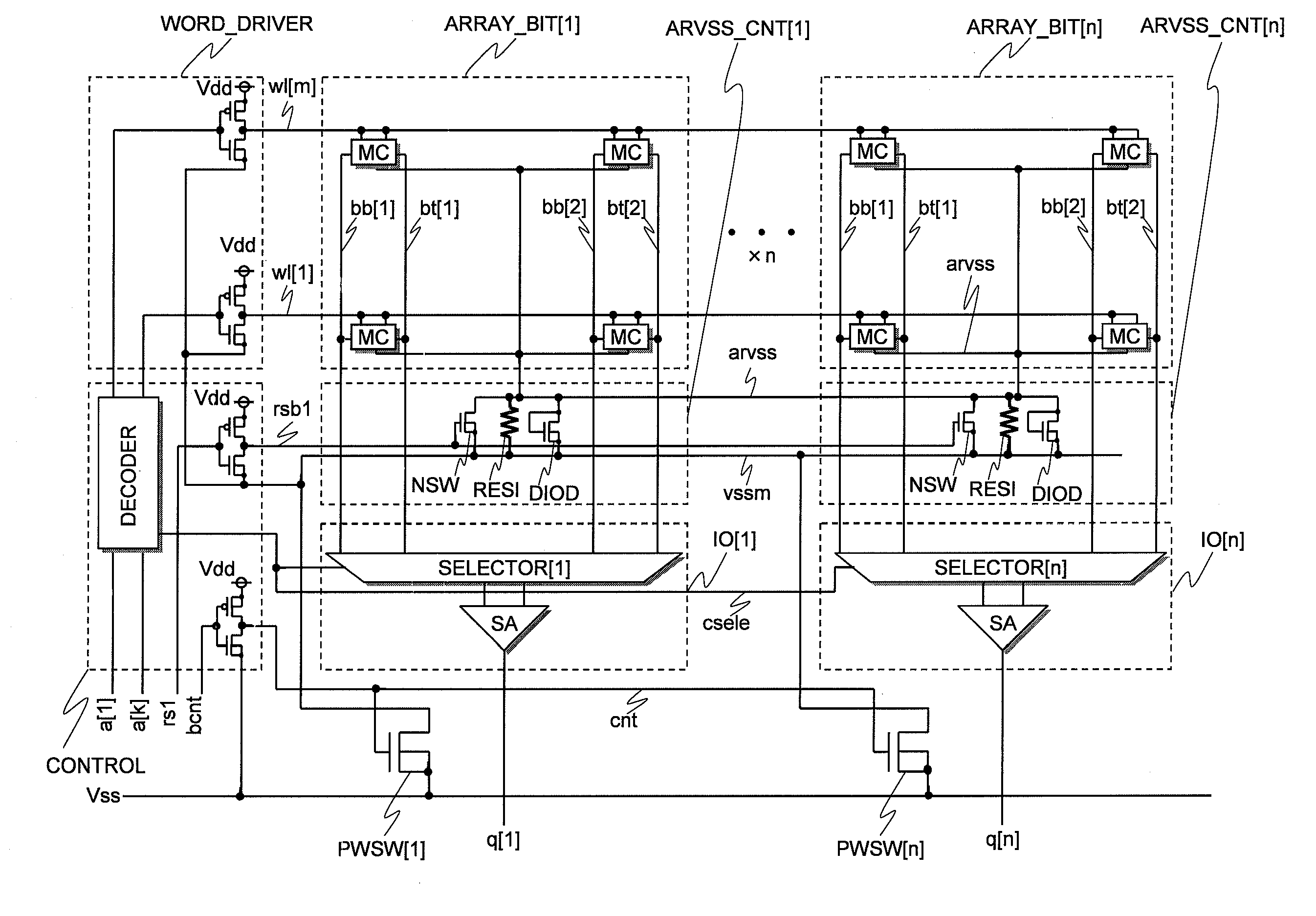
[0104]FIG. 5 illustrates a configuration of a semiconductor integrated circuit according to Embodiment 1 of the present invention.

[0105]A semiconductor integrated circuit according to Embodiment 1 of the present invention illustrated in FIG. 5 is different from the semiconductor integrated circuit illustrated in FIG. 2, examined by the present inventors in advance of the present invention, in the following points.

[0106]That is, in the semiconductor integrated circuit according to Embodiment 1 of the present invention illustrated in FIG. 5, a power switch PWSW22 is coupled between a local power source vssm22 of an SRAM module (SRAM2) and a ground potential Vss, a control signal cnt22 is supplied to a control gate of the power switch PWSW22; a power switch PWSW23 is coupled between a local power source vssm23 of an SRAM module (SRAM3) and the ground potential Vss, and a control signal cnt23 is supplied to a...

embodiment 2

A Configuration of a Semiconductor Integrated Circuit According to Embodiment 2

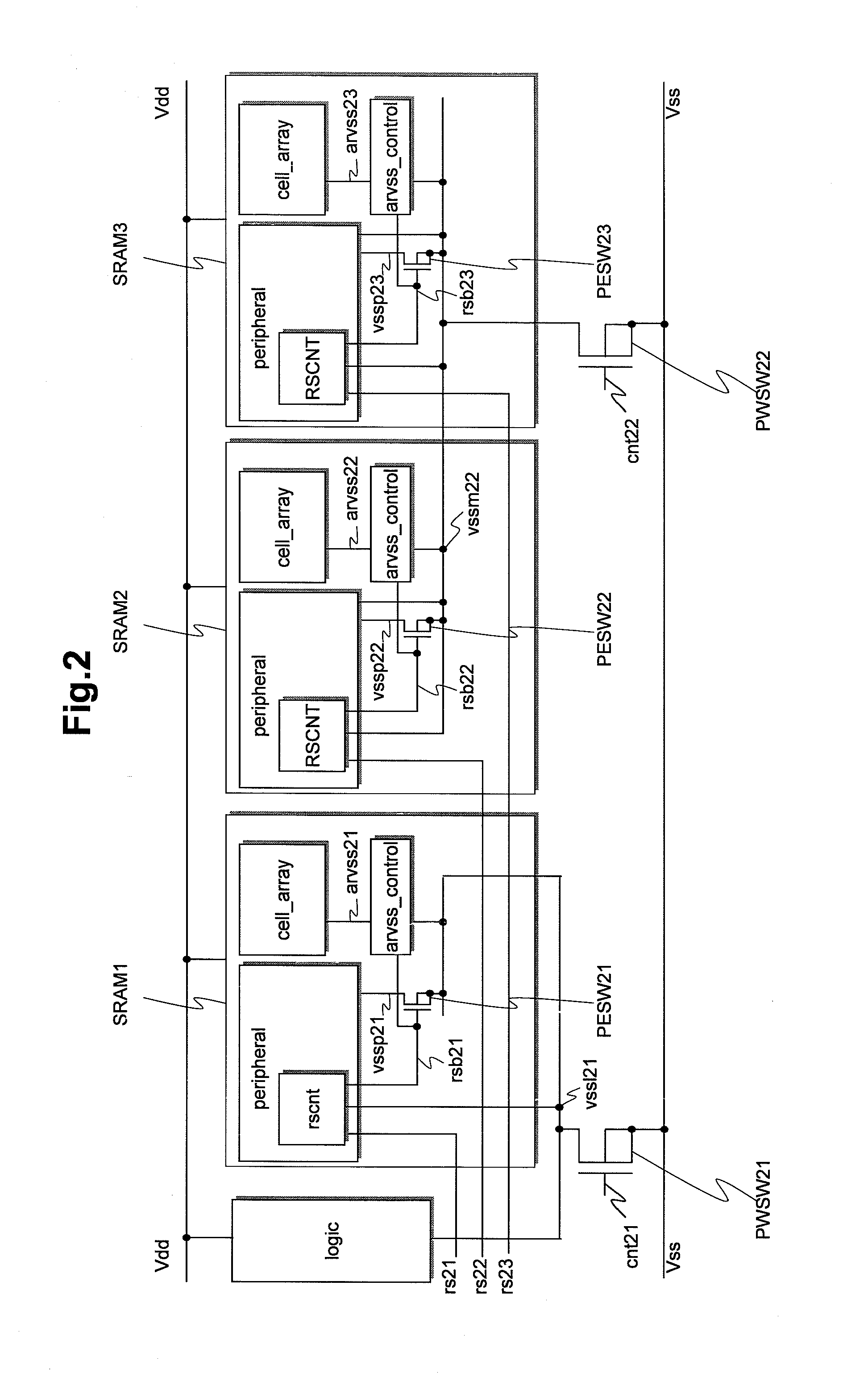
[0140]FIG. 11 illustrates a configuration of a semiconductor integrated circuit according to Embodiment 2 of the present invention.

[0141]A semiconductor integrated circuit according to Embodiment 2 of the present invention illustrated in FIG. 11 is different from the semiconductor integrated circuit according to Embodiment 1 of the present invention illustrated in FIG. 5 in the following points.

[0142]That is, in the semiconductor integrated circuit according to Embodiment 2 of the present invention illustrated in FIG. 11, a local power line of the second SRAM module (SRAM2) and a local power line of the third SRAM module (SRAM3) share the second local power line vssm22. Furthermore, the second power switch PWSW22 and the third power switch PWSW23 which are coupled between the shared second local power line vssm22 and the ground potential Vss are shared by the second SRAM module (SRAM2) and the third SRAM ...

embodiment 3

A Configuration of a Semiconductor Integrated Circuit According to Embodiment 3

[0175]FIG. 14 illustrates a configuration of a semiconductor integrated circuit according to Embodiment 3 of the present invention.

[0176]A semiconductor integrated circuit according to Embodiment 3 of the present invention illustrated in FIG. 14 is different from the semiconductor integrated circuit according to Embodiment 2 of the present invention illustrated in FIG. 11 in the following points.

[0177]The first difference is that the switches MSW21, MSW22, and MSW23, each comprising the N-channel MOS transistor of the source line potential control circuit of three SRAM modules (SRAM1, SRAM2, SRAM3) of the semiconductor integrated circuit according to Embodiment 2 of the present invention illustrated in FIG. 11, are replaced by switches MPSW21, MPSW22, and MPSW23, each comprising a P-channel MOS transistor of a source line potential control circuit of the semiconductor integrated circuit according to Embod...


PUM


Abstract

A semiconductor integrated circuit which can respond to changes of the amount of retained data at the time of standby is provided. The semiconductor integrated circuit comprises a logic circuit (logic) and plural SRAM modules. The plural SRAM modules perform power control independently of the logic circuit, and an independent power control is performed among the plural SRAM modules. Specifically, one terminal and the other terminal of a potential control circuit of each SRAM module are coupled to a cell array and a local power line, respectively. The local power line of one SRAM module and the local power line of the other SRAM module share a shared local power line. A power switch of one SRAM module and a power switch of the other SRAM module are coupled in common to the shared local power line.

Description

CLAIM OF PRIORITY[0001]The present application claims priority from Japanese patent application JP 2009-211335 filed on Sep. 14, 2009, and the content of which is hereby incorporated by reference into this application.FIELD OF THE INVENTION[0002]The present invention relates to a semiconductor integrated circuit and an operation method for the same, especially to technology which is effective in responding to changes of the amount of retained data in a standby state.BACKGROUND OF THE INVENTION[0003]According to miniaturization in a semiconductor manufacturing process, the number of MOSFETs which are integrated in a single LSI (LSI: Large Scale Integrated circuits) has increased, with an accompanied increase of leakage current. Especially in the mobile use, under the limited battery capacity, a system on a chip (SoC) of this family needs to satisfy a demand for a strict leakage current. According to Non-patent Document 1 cited below, the effective method in such a situation is cuttin...

Claims


Application Information

Patent Timeline
IPC IPC(8): G11C11/417G11C11/412G11C5/14
CPCH01L27/1104G11C5/06G11C5/14G11C11/413H01L27/092H10B10/12G11C11/417
Inventor KOMATSU, SHIGENOBUYAMAOKA, MASANAOMAEDA, NORIAKIMORIMOTO, MASAOSHIMAZAKI, YASUHISAOKUMA, YASUYUKISANO, TOSHIAKI
Owner RENESAS ELECTRONICS CORP
Why Eureka
Try Eureka