

Method of manufacturing light emitting diode packaging lens and light emmiting diode package
a technology of light-emitting diodes and packaging lenses, which is applied in the direction of superimposed coating processes, solid-state devices, coatings, etc., can solve the problems of non-uniform phosphor distribution in the glue, annular yellow rings, and non-uniform reradiation of blue light and annular rings
- Summary
- Abstract
- Description
- Claims
- Application Information
AI Technical Summary
Problems solved by technology
Method used
Image

Examples
first embodiment
[0064]Please refer to FIG. 6 to FIG. 21. A first embodiment is illustrated. FIG. 6 shows a schematic cross-sectional view of a cup 100. The cup 100 is transparent and made of polycarbonate (PC). It has a diameter of 4.5 mm and uniform thickness of 0.5 mm. The cup 100 has a shape of hemisphere. It means that a point A on FIG. 6 keeps equally distant from each part of the concave surface of the cup 100. A transparent conductive coating layer 102 is formed on the concave surface of the cup 100 and made of indium tin oxide (ITO). ITO particles are sputtered onto the cup 100. Since ITO is transparent and conductive, its thickness can be 200-300 nm in practice.
[0065]Shown in FIG. 7 is an electrophoretic deposition tank 200 used in the first embodiment. The tank 200 contains a first solution 202 which comprises a first group of phosphors (not shown). In this embodiment, the phosphor particles used are Y3A15O12 (YAG):Ce. YAG particles stay in a suspension status in the first solution 202. A...
second embodiment
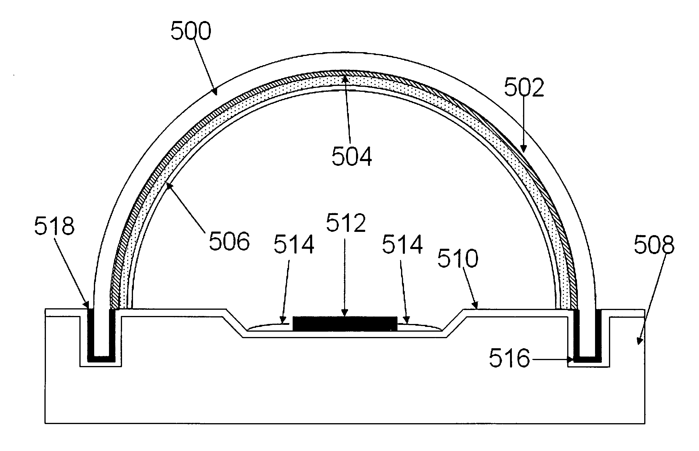
[0077]Please refer FIG. 22 and FIG. 23. A second embodiment is illustrated. A cup 500 which is transparent and has a hemispheric portion 5002 and a short cylinder portion 5004. The cup 500 is made of polymethyl methacrylate (PMMA). Its size is 5.0 mm and has uniform thickness of 0.5 mm. A transparent conductive coating layer 502 is formed on the concave surface of the cup 500 and made of indium zinc oxide (IZO). IZO particles are sputtered onto the cup 500. Since IZO is transparent and conductive, its thickness can be 200-300 nm in practice. By using the same process, solvent and binder of electrophoretic deposition in the first embodiment, a phosphor layer 504 is formed. Here, a Terbium-doped YAG and a Cerium-doped YAG are used as phosphors. During the electrophoretic deposition process, the phosphors combine with magnesium ions and become cations. Therefore, they can be coated on the cathode side.
[0078]Then, a gel-like fixing liquid is sprayed over the concave surface of the cup 5...
third embodiment
[0080]According to the present invention, number of the phosphor layer is not limited to one. For a specific color light, two or more layers of phosphors can be applied. It can be achieved by electrophoretic deposition, too.
[0081]Please see FIG. 24. A third embodiment is illustrated. A cup 600 which is transparent and hemispherical and made of glass. A transparent conductive coating layer 602 is formed on the concave surface of the cup 600 and made of aluminum zinc oxide (AZO). AZO particles are sputtered onto the cup 600. By using the same process, solvent and binder of electrophoretic deposition in the first embodiment, a first phosphor layer 604 is formed. Here, the first phosphor layer 604 has MgSiO3:Eu phosphors for generating a red light by excitation of LED light. Then, the cup 600 is removed from the first solution described in the first embodiment and immersed into a second solution. The second solution has Cerium-doped YAG phosphors, solvent of IPA and binder of silver nit...
PUM
| Property | Measurement | Unit |
|---|---|---|
| Thickness | aaaaa | aaaaa |
| Shape | aaaaa | aaaaa |
| Radius | aaaaa | aaaaa |
Abstract
Description
Claims
Application Information