Method for making trench MOSFET with shallow trench structures

a technology of trench mosfet and shallow trench structure, which is applied in the field of cell configuration and fabrication process of power mosfet devices, can solve problems such as breakdown voltage degradation, and achieve the effects of avoiding over-etching, preventing gate/drain shortage, and avoiding breakdown voltage degradation

Inactive Publication Date: 2011-03-24
MEMOIR SYST +1
View PDF32 Cites 21 Cited by
  • Summary
  • Abstract
  • Description
  • Claims
  • Application Information

AI Technical Summary

Benefits of technology

[0010]Another aspect of the present invention is that, shallow trenched gates are formed with thick bottom insulation layer, for example, with thick bottom oxide by oxidizing un-doped poly silicon (deposited at 650° C. or above) or amorphous silicon (deposited below 650° C.) on top of gate oxide at trench bottom. By employing this structure, the Qgd of the trench MOSFET can be further reduced without having degradation of breakdown voltage due to the bird's beak effect of the prior art.
[0011]Another aspect of the present invention is that, in fabrication process, source-body contact trenches and gate contact trenches are defined by two different contact masks to avoid over-etching issue which happens when

Problems solved by technology

Another disadvantage of prior art is that, as illustrated in FIG. 2 (the upper curve), to prevent the increase of Rds (Resistance between Drain and Source), a difference between Td (Trench Depth, FIG. 1A) and Pd (P body depth, FIG. 1A) must be kept larger than 0.4 μm, thus forming a large overlap region between gate and epitaxial layer, therefore greatly i

Method used


Image

  • Method for making trench MOSFET with shallow trench structures
  • Method for making trench MOSFET with shallow trench structures
  • Method for making trench MOSFET with shallow trench structures

Examples


Embodiment Construction

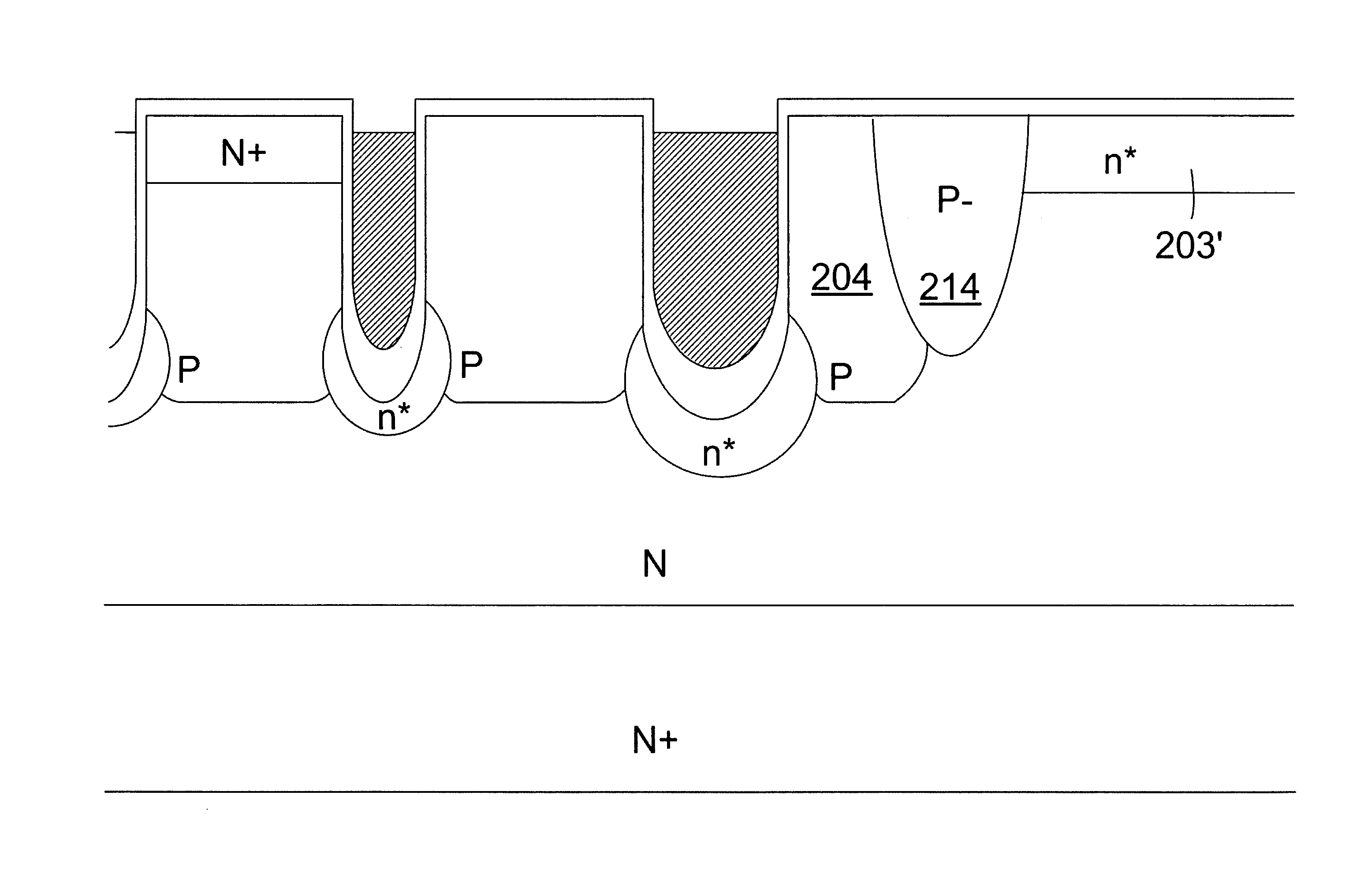
[0030]Please refer to FIG. 4 for a preferred embodiment of this invention where an N-channel trench MOSFET with shallow trench structures is formed on a heavily N+ doped substrate 200 onto which a lightly N doped epitaxial layer 201 is grown. A plurality of shallow trenched gates are formed within said epitaxial layer and filled with doped poly onto gate oxide 202 to form shallow trenched gates 210 and at least a wider shallow trenched gate 211 for gate connection. What should be noticed is that, oxide layer on the bottom of each of trenched gates 210 and 211 is thicker than that along the sidewalls. Around the bottom of each trenched gate 210 and 211, an n* is formed with heavier concentration than said epitaxial layer. N+ source region 205 is formed near the top surface of P body region 204 between every two adjacent shallow trenched gates 210. The shallow trench MOSFET further comprises: trenched source-body contact filled with tungsten plug 208 penetrating through an insulation ...


PUM


Abstract

A method for making trench MOSFET with shallow trench structures with thick trench bottom is disclosed. The improved method resolves the problem of deterioration of breakdown voltage resulted by LOCOS having a bird's beak shape introduced in prior art, and at the same time, the inventive device has a lower Qgd and lower Rds.

Description

BACKGROUND OF THE INVENTION[0001]1. Field of the Invention[0002]This invention relates generally to the cell configuration and fabrication process of Power MOSFET devices. More particularly, this invention relates to a novel and improved trench MOSFET cell structure, and improved process of fabricating a trench MOSFET with shallow trench structures.[0003]2. The Prior Arts[0004]In order to resolve restrict of high gate charge introduced in trench MOSFET of conventional configurations, shallow trench structure was disclosed by decreasing trench depth, please refer to FIG. 1A for an N-channel trench MOSFET of prior art. However, when etching the shallow trench during fabrication process, the trenched gate contact 109 into shallow trenched gate may penetrate through gate oxide and short to drain because the Cdpoly (trenched gate contact depth, as shown in FIG. 1A) is about 1.5 times deeper than Cdsi (trenched source-body contact depth into epitaxial layer, as shown in FIG. 1A) as the re...

Claims


Application Information

Patent Timeline
IPC IPC(8): H01L21/336H01L21/28
CPCH01L29/0615H01L29/0619H01L29/0878H01L29/1095H01L29/41766H01L29/7813H01L29/42368H01L29/66719H01L29/66727H01L29/66734H01L29/7811H01L29/4236
Inventor HSIEH, FU-YUAN
Owner MEMOIR SYST
Why Eureka
Try Eureka