Method for manufacturing trench metal-oxide semiconductor field effect transistor (MOSFET)

A technology of oxide semiconductors and field effect transistors, which is applied in semiconductor/solid-state device manufacturing, semiconductor devices, transistors, etc., can solve problems such as over-etching, enlargement, metal plug and drain short circuit, and reduce Qgd , Rds is small, the effect of reducing Rds

Inactive Publication Date: 2013-12-04
FORCE MOS TECH CO LTD
View PDF1 Cites 0 Cited by
  • Summary
  • Abstract
  • Description
  • Claims
  • Application Information

AI Technical Summary

Problems solved by technology

However, in the process of etching the contact trench, since the etching rate of polysilicon is greater than that of single crystal silicon, it is easy to cause the depth Cdpoly of the gate contact trench (such as Figure 1A shown) is approximately the depth Cdsi of the source-body contact trench (eg Figure 1A 1.5 times as shown)
At the same time, since the depth of the trench gate in the epitaxial layer is reduced, over-etching is very easy to occur when the gate contact trench 109 is etched, that is, the bottom of the gate contact trench 109 extends into the epitaxial layer in a conventional trench gate. resulting in a short circuit between the metal plug in the gate contact trench 109 and the drain
[0003] Another deficiency of the existing technology is that, from the analysis of experimental data, such as figure 2 As shown in the upper curve, in order to avoid the increase of the source-drain resistance Rds, the depth Td of the trench gate (such as Figure 1A shown) and the depth Pd of the body region (such as Figure 1A shown) must be greater than 0.4μm, and this will cause an increase in the area of ​​direct contact between the trench gate and the epitaxial layer, resulting in a gate-to-drain charge Qgd (such as Figure 1A shown) increase
However, the thicker oxide layer 129 at the bottom of the trench gate is formed by local oxidation of silicon (LOCOS) at the bottom of the trench, so there is a Bird's Beak at the bottom of the sidewall nitride 130 region 131, which causes the gate oxide at the bottom corners of the trench gate to be too weak causing a reduction in breakdown voltage

Method used


Image

  • Method for manufacturing trench metal-oxide semiconductor field effect transistor (MOSFET)
  • Method for manufacturing trench metal-oxide semiconductor field effect transistor (MOSFET)
  • Method for manufacturing trench metal-oxide semiconductor field effect transistor (MOSFET)

Examples


Embodiment Construction

[0054] The invention will be described in detail below with reference to the accompanying drawings, in which preferred embodiments of the invention are shown. The invention can, however, be embodied in different ways and should not be limited to the embodiments described herein. For example, the description here refers more to N-channel trench MOSFETs, but clearly other devices are possible.

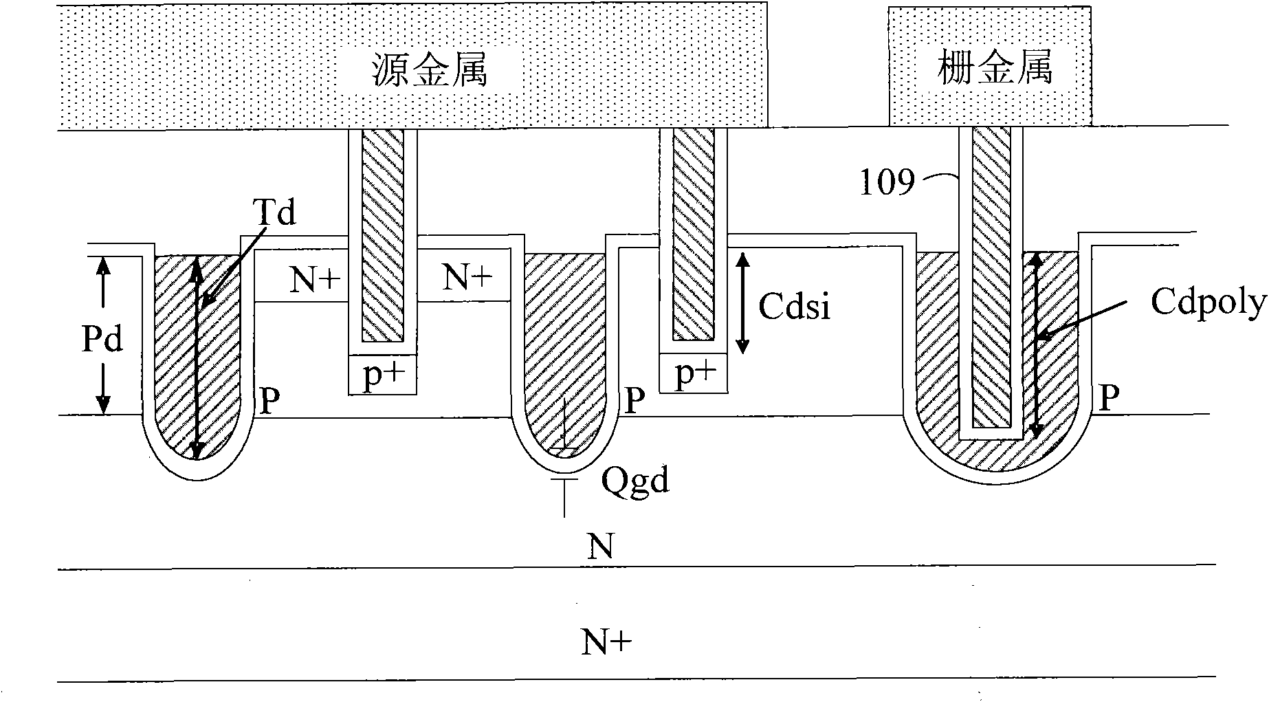
[0055] refer to Figure 4 Shown is an N-channel shallow trench MOSFET according to a preferred embodiment of the present invention. The N-type epitaxial layer 201 is formed on the N+ substrate 200, and the inner surface of multiple trenches formed in the epitaxial layer is lined with a gate oxide layer 202 and filled with doped polysilicon to form multiple trench gates 210 and At least one wider trench gate 211, wherein the at least one wider trench gate 211 is used to connect gate metal. In particular, the thickness of the gate oxide layer 202 at the bottom of each trench is greater ...


PUM


Abstract

The invention discloses a method for manufacturing a trench metal oxide semiconductor field effect transistor (MOSFET). According to the trench MOSFET provided by the invention, the bottom of a trench grid in the epitaxial layer of the trench MOSFET has a thicker insulation layer compared with the side wall of the trench grid. The manufacture method provided by the invention avoids a bird beak effect generated by the thicker insulation layer at the bottom of the trench grid growing by utilizing a LOCOS (Local Oxidation Of Silicon) method in the prior art. Meanwhile, a shallow trench MOSFET based on the invention has lower Qgd (Grid Drain Charge) and lower Rds (Resource Drain Charge).

Description

technical field [0001] The invention relates to a unit structure, device structure and process manufacturing of a semiconductor power device, in particular to a unit structure and a process method of a trench MOSFET (Metal Oxide Semiconductor Field Effect Transistor). Background technique [0002] In order to solve the problem that the traditional trench metal-oxide-semiconductor field-effect transistor (MOSFET) has a relatively high gate charge, the prior art discloses a method of reducing the gate depth by reducing the depth of the trench gate (hereinafter referred to as shallow trench MOSFET). Charge shallow trench MOSFET structures, such as Figure 1A The N-channel Trench MOSFET shown. However, in the process of etching the contact trench, since the etching rate of polysilicon is greater than that of single crystal silicon, it is easy to cause the depth Cdpoly of the gate contact trench (such as Figure 1A shown) is approximately the depth Cdsi of the source-body contact...

Claims


Application Information

Patent Timeline
Patent Type & Authority Patents(China)
IPC IPC(8): H01L21/8234H01L21/336H01L27/088H01L29/78H01L29/06
CPCH01L29/0878H01L29/41766H01L29/7811H01L29/7813
Inventor 谢福渊
Owner FORCE MOS TECH CO LTD
Why Eureka
Try Eureka