Semiconductor device

a technology of semiconductor chips and semiconductor components, applied in the manufacture of printed circuits, printed circuit aspects, basic electric elements, etc., can solve the problems of deterioration in reliability, increased problems of deterioration in external packageability, and chip or characteristic breakage, so as to prevent the warpage of semiconductor chips

Inactive Publication Date: 2011-03-31
ELPIDA MEMORY INC
View PDF87 Cites 24 Cited by
  • Summary
  • Abstract
  • Description
  • Claims
  • Application Information

AI Technical Summary

Benefits of technology

[0012]According to this invention, a support is provided on a wiring board for supporting a semiconductor chip and for forming a gap between the semiconductor chip and the wiring board, whereby a sealing resin can be arranged in a similar manner on both of the opposite surfaces of the semiconductor chip. This makes it possible to substantially equalize the physical property values between the opposite surfaces of the semiconductor chip, and thus to prevent the warpage of the semiconductor chip.

Problems solved by technology

This type of semiconductor devices is susceptible to such a problem that warpage is caused by a difference in coefficient of thermal expansion between semiconductor chip and wiring board.
For example, difference in physical property values between one surface and the other surface of a semiconductor chip may cause warpage (or stress), leading to breakage of the chip or deterioration in characteristics even if the chip is not broken.
Thus, there have been increased problems of deterioration in reliability.
In addition, there have been increased problems of deterioration in external packageability caused by warpage in an entire package.
Therefore, this semiconductor device still has problems of deterioration in reliability and poor external packageability.
However, no consideration at all is given, in this semiconductor device, to warpage in the semiconductor chip or in the entire package.
However, no consideration is given, in this semiconductor device, to warpage in the semiconductor chip or in the entire package.

Method used


Image

  • Semiconductor device
  • Semiconductor device
  • Semiconductor device

Examples


first embodiment

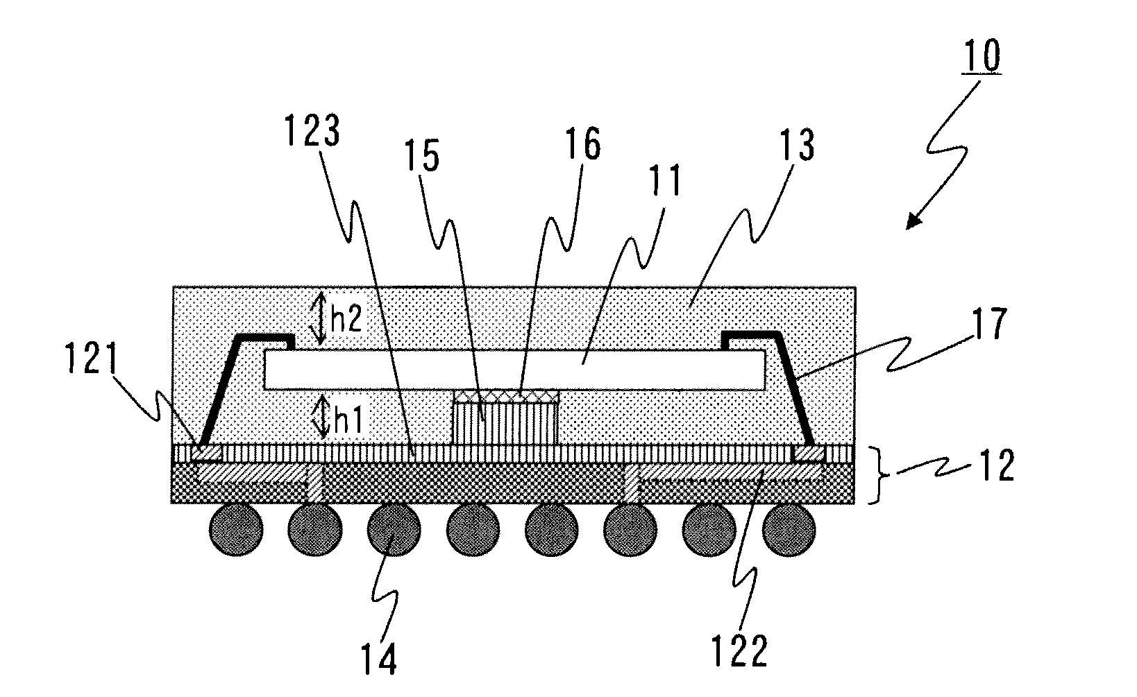
[0022]FIG. 1 shows a configuration in cross section of a semiconductor device 10 according to this invention, and FIG. 2 is a plan transparent view thereof.

[0023]As seen from FIG. 1, this semiconductor device 10 is a BGA (Ball Grid Array) type semiconductor device. The semiconductor device 10 has a semiconductor chip 11, a wiring board 12 on which the semiconductor chip 11 is mounted, and a sealing resin 13 sealing the semiconductor chip 11 on the wiring board 12.

[0024]The wiring board 12 is, for example, a glass epoxy board having external dimensions slightly greater than those of the semiconductor chip 11. There are formed, on one surface (upper surface) of the wiring board 12, a plurality of connection pads 121 made for example of gold (Au) or copper (Cu), and predetermined wirings 122 connected to the connection pads 121. A solder resist (insulation film) 123 is formed to cover the wirings 122. The solder resist 123 serves to prevent removal of the wiring 122 as well as to avoid...

second embodiment

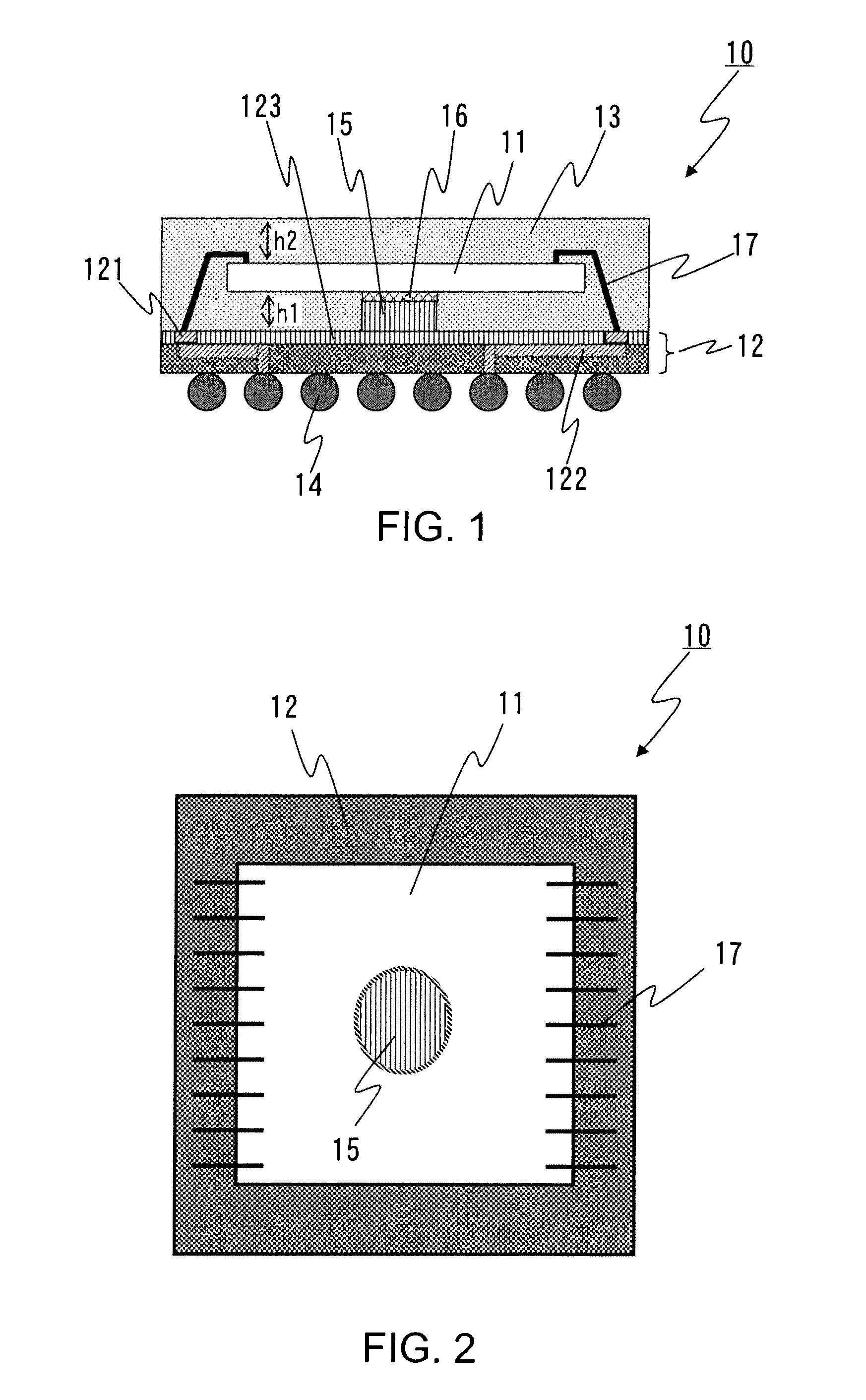
[0038]Next, referring to FIG. 4, a semiconductor device according to this invention will be described.

[0039]FIG. 4 is a plan transparent view as seen from above the semiconductor device according to this second embodiment. The shown semiconductor device has the same configuration as that of the semiconductor device according to the first embodiment except that the semiconductor device according to the second embodiment has projections 15a as a support instead of the projection 15 in the semiconductor device according to the first embodiment. Therefore, description of the configuration will be omitted.

[0040]The projections 15a include a first projection 15-1 which is a circular cylindrical member provided in a central part of a semiconductor chip mounting region, and second projections 15-2 consisting of four rectangular parallelepiped members (members with a substantially rectangular cross section) extending radially from the central part to four corners. Each corner of the second p...

third embodiment

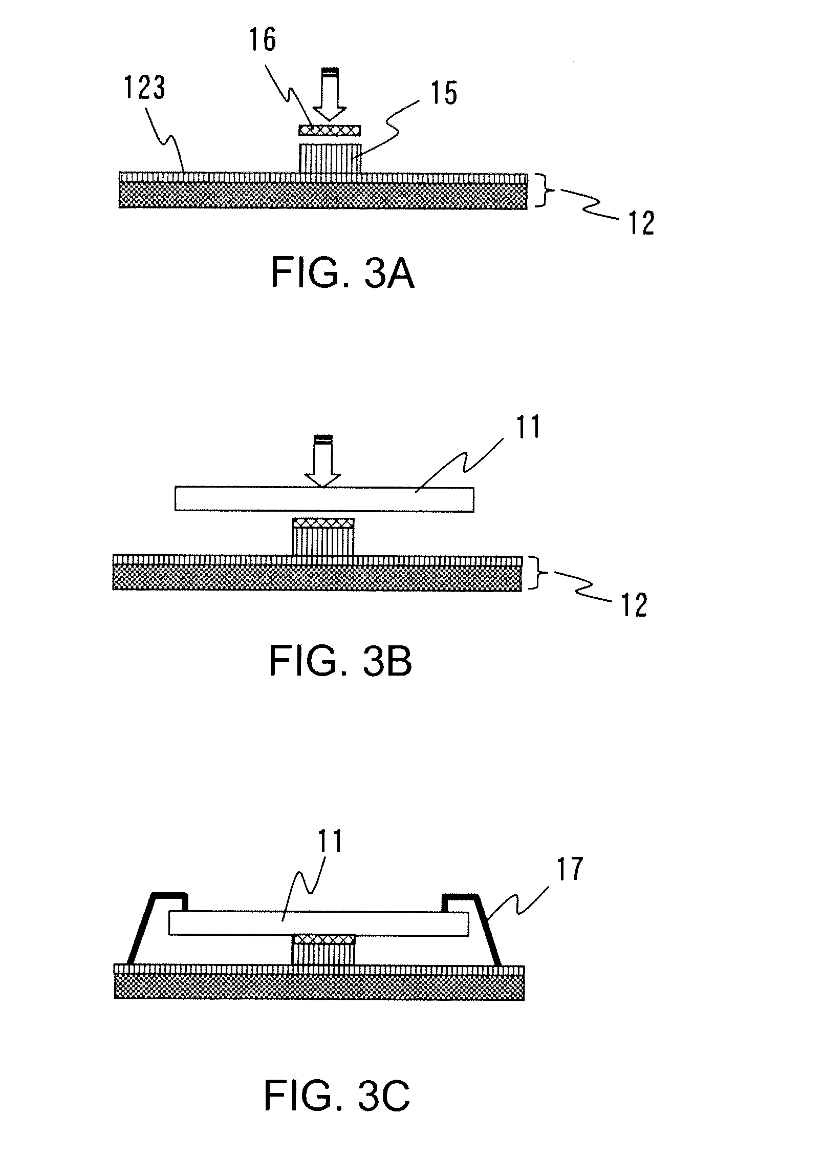
[0042]Next, referring to FIG. 5, a semiconductor device according to this invention will be described.

[0043]FIG. 5 is a plan transparent view of the semiconductor device according to this embodiment as seen from the above. The shown semiconductor device has a pair of projections 15b in place of the projection 15 in the semiconductor device according to the first embodiment. Except for the projections 15b, the semiconductor device according to the third embodiment has the same configuration as that of the semiconductor device according to the first embodiment, and hence description thereof will be omitted.

[0044]As shown in FIG. 5, the pair of projections 15b are rectangular parallelepiped members arranged along two parallel sides of the semiconductor chip. Each corner of the projections 15b may be rounded.

[0045]According to this embodiment, the semiconductor chip 11 is fixed stably along the two parallel sides in the outer periphery of the chip. This enables a stable wire bonding pro...


PUM


Abstract

A device has a semiconductor chip, a wiring board, a support which supports the semiconductor chip on the wiring board and forms a gap between the semiconductor chip and the wiring board, and a sealing resin injected into the gap and covering the semiconductor chip.

Description

[0001]This application is based upon and claims the benefit of priority from Japanese patent application No. 2009-224322, filed on Sep. 29, 2009, the disclosure of which is incorporated herein in its entirety by reference.BACKGROUND OF THE INVENTION[0002]This invention relates to a semiconductor device and, in particular, to a semiconductor device in which a semiconductor chip is mounted on a wiring board and sealed with a resin.[0003]CSP (Chip Size Package) or other types of semiconductor devices typically have a semiconductor chip mounted on a wiring board and sealed with resin. This type of semiconductor devices is susceptible to such a problem that warpage is caused by a difference in coefficient of thermal expansion between semiconductor chip and wiring board.[0004]In order to solve such a problem, a related semiconductor device is designed to have a contact area between semiconductor chip and wiring board smaller than the area of the semiconductor chip, so that a first region ...

Claims


Application Information

Patent Timeline
Patent Type & Authority Applications(United States)
IPC IPC(8): H01L23/48
CPCH01L23/3128H01L23/3135H01L23/49816H01L24/29H01L24/32H01L24/45H01L24/48H01L24/83H01L25/105H01L2224/32014H01L2224/32225H01L2224/45144H01L2224/45147H01L2224/48095H01L2224/48227H01L2224/49175H01L2224/73265H01L2224/83192H01L2224/838H01L2224/92247H01L2924/01002H01L2924/01004H01L2924/01005H01L2924/01014H01L2924/01029H01L2924/01079H01L2924/01082H01L2924/078H01L2924/15311H01L2924/15331H01L2924/3511H05K3/284H05K3/305H05K2201/2036H05K2203/049H01L2224/2919H01L2924/01006H01L2924/01033H01L2924/014H01L2924/0665H01L24/27H01L2224/83101H01L24/49H01L2225/1023H01L2225/1058H01L2924/07802H01L2924/00014H01L2924/00H01L2924/3512H01L2924/00012H01L2924/181H01L24/73H01L2224/32055H01L2224/83385
Inventor TAKESHIMA, HIDEHIROINAKAWA, SUSUMU
Owner ELPIDA MEMORY INC
Why Eureka
Try Eureka