Imaging device and electronic camera

a technology of electronic camera and imaging device, which is applied in the field of imaging device and electronic camera, can solve the problems of remarkable reduction of focus detection precision, increase of microlens focal length, and light incident amount, and achieve the effects of low cost, low cost, and high detection accuracy

Inactive Publication Date: 2011-03-31
FUJIFILM CORP
View PDF7 Cites 67 Cited by
  • Summary
  • Abstract
  • Description
  • Claims
  • Application Information

AI Technical Summary

Benefits of technology

[0007]An arrayed configuration in which a plurality of photographic elements and a plurality of phase difference detection elements are disposed on a light receiving surface can eliminate the need to use an optical path dividing mechanism and a distance measuring sensor and thus achieve low costs and space saving as well as high-speed focus detection. However, further microfabrication reduces the amount of light incident on a photoelectric conversion element. In particular, the phase difference detection element group performs photoelectric conversion on object light passing through a partial region of the exit pupil of the photographic lens, and thus a reduction in incident light causes a remarkable reduction in focus detection precision.
[0008]Note that as disclosed in Japanese Patent Application Laid-Open No. 2008-71920, when a microlens is disposed for a plurality of photoelectric conversion elements for phase difference detection, the focal length of the microlens increases and thus it is difficult to dispose the photoelectric conversion elements for phase difference detection and the photoelectric conversion element for photographing on the same plane. Moreover, when the photoelectric conversion elements for a microlens are divided into one for phase difference detection and one for photographing, further microfabrication makes it difficult to form an opening thereof in such a manner that one for guiding light into the photoelectric conversion element for phase difference detection is smaller than one for the photoelectric conversion element for photographing. Moreover, the amount of light incident on a photoelectric conversion element is reduced remarkably.

Problems solved by technology

However, further microfabrication reduces the amount of light incident on a photoelectric conversion element.
In particular, the phase difference detection element group performs photoelectric conversion on object light passing through a partial region of the exit pupil of the photographic lens, and thus a reduction in incident light causes a remarkable reduction in focus detection precision.
Note that as disclosed in Japanese Patent Application Laid-Open No. 2008-71920, when a microlens is disposed for a plurality of photoelectric conversion elements for phase difference detection, the focal length of the microlens increases and thus it is difficult to dispose the photoelectric conversion elements for phase difference detection and the photoelectric conversion element for photographing on the same plane.
Moreover, when the photoelectric conversion elements for a microlens are divided into one for phase difference detection and one for photographing, further microfabrication makes it difficult to form an opening thereof in such a manner that one for guiding light into the photoelectric conversion element for phase difference detection is smaller than one for the photoelectric conversion element for photographing.
Further, if an internal structure is made differently between the photographic element and the phase difference detection element, it is difficult to reuse the internal structure for ordinary imaging device, causing another problem with an increase in manufacturing cost in the entire business.
Furthermore, the photoelectric conversion element (pixel) for phase difference detection is subject to a restriction in a light receiving direction and thus it is difficult to use the pixel information to generate high-quality photographic image data.
Still furthermore, when phase difference detection elements are disposed at high density in order to ensure focus detection precision at low intensity, the photographic image quality deteriorates.

Method used


Image

  • Imaging device and electronic camera
  • Imaging device and electronic camera
  • Imaging device and electronic camera

Examples


first embodiment

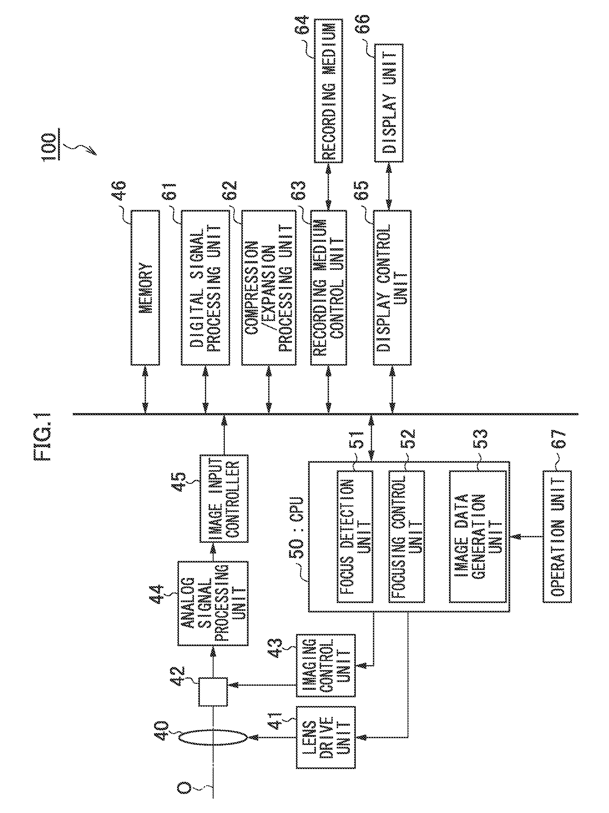
[0082]First, an imaging unit 42 will be described. Note that what has been described by referring to FIGS. 2 to 4 will be omitted here.

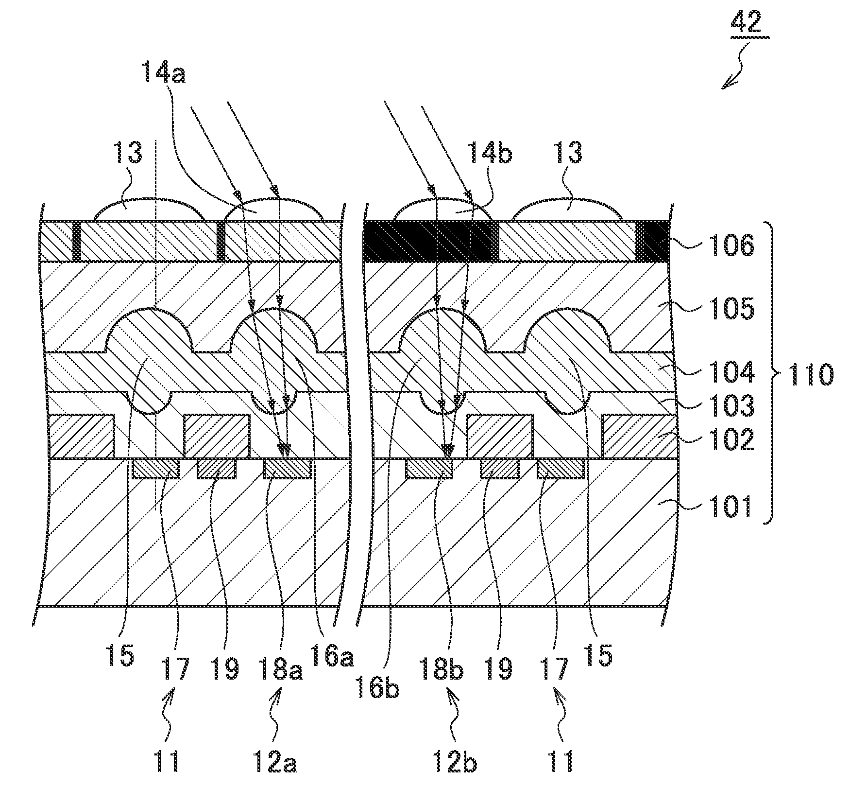
[0083]FIG. 5 is a sectional view illustrating a phase difference detection element 12 according to the first embodiment. As illustrated in FIG. 5, the phase difference detection element 12 according to the present embodiment is configured such that the optical axis (central axis) of the top microlens 14 is shifted from the optical axis (central axis) of the inner microlens 16. In addition, the optical axis of the inner microlens 16 is shifted from the optical axis of the photodiode 18. Further, the optical axis of the top microlens 14 is shifted from the optical axis of the photodiode 18.

[0084]The present embodiment is configured such that the optical axis of the top microlens 14 is shifted from the optical axis of the inner microlens 16. Thus, the photodiode 18 can efficiently receive object light passing through a partial region of the exit pupil ...

fourth embodiment

[0090]Next, an imaging unit 42 will be described. Note that what has been described by referring to FIGS. 2 to 4 will be omitted here.

[0091]FIG. 8 is a sectional view illustrating a phase difference detection element 12 according to the present embodiment. As illustrated in FIG. 8, the phase difference detection element 12 according to the present embodiment is configured such that the optical axis (central axis) of the entrance lens 161 of the inner microlens 16 is shifted from the optical axis (central axis) of the exit lens 162. The entrance lens 161 is a convex lens (upper convex lens) on an upstream side of the optical path, and the exit lens is a convex lens (lower convex lens) on a downstream side of the optical path.

[0092]Note that the present embodiment is further configured such that the optical axis of the top microlens 14 is shifted from the optical axis of the entrance lens 161 of the inner microlens 16. Furthermore, the optical axis of the entrance lens 161 of the inn...

sixth embodiment

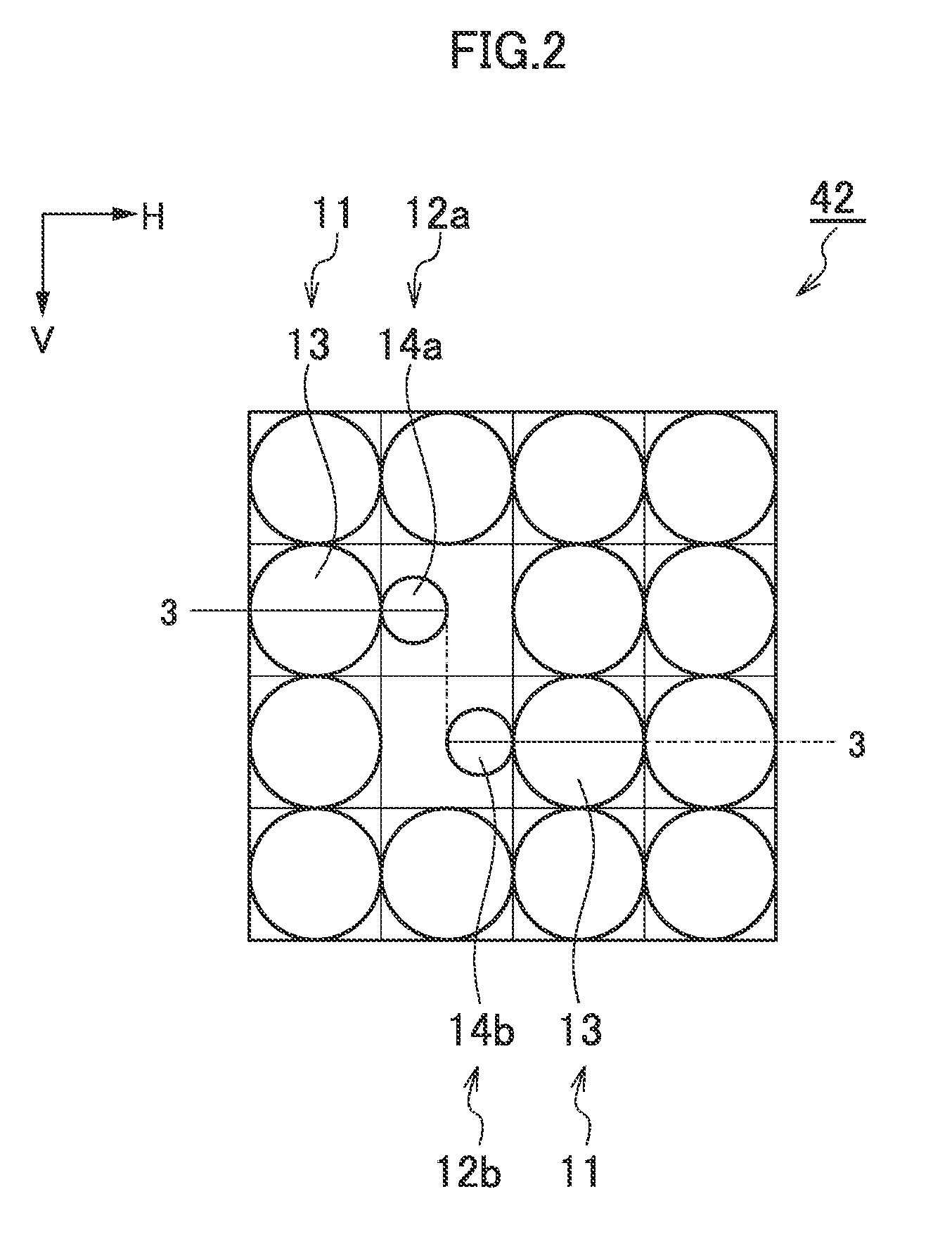
[0098]FIG. 10 is a plan view illustrating an element arrangement of an imaging unit 42 according to a As illustrated in FIG. 10, in the present embodiment, phase difference detection element pairs 31 having a mutually adjacent first phase difference detection element 12a and second phase difference detection element 12b are arranged in an array pattern along the horizontal direction H which is a phase difference detection direction.

[0099]In FIG. 10, each of R, G, and B designates a color of the color filter. The photographic element 11 has a color filter of R (red), G (green) or B (blue), and the phase difference detection elements 12 (12a and 12b) has a color filter of G. In addition, three photographic elements 11 having a color filter of the same color (G in the present embodiment) are arranged adjacent to each phase difference detection element 12. One (e.g., 11a) of the photographic elements 11 is located between the phase difference detection element pairs 31. For example, th...


PUM


Abstract

An imaging device includes an arrayed imaging element group configured to receive light passing through a photographic lens, wherein the imaging element group includes a plurality of photographic elements used for photographic image data generation and a plurality of phase difference detection elements used for phase difference detection for focus detection of the photographic lens, each of the photographic elements and each of the phase difference detection elements include: an on-chip microlens configured to collect light passing through the photographic lens; a photoelectric conversion element configured to receive the light passing through the on-chip microlens; and an internal microlens disposed between the on-chip microlens and the photoelectric conversion element, the photographic element is configured such that an optical axis of the on-chip microlens matches an optical axis of the internal microlens, and the phase difference detection element is configured such that the optical axis of the on-chip microlens is shifted from the optical axis of the internal microlens.

Description

BACKGROUND OF THE INVENTION[0001]1. Field of the Invention[0002]The presently disclosed subject matter relates to an imaging device having an imaging element group used for photographic image data generation and an imaging element group used for phase difference detection; and an electronic camera having the imaging device.[0003]2. Description of the Related Art[0004]There has been known an imaging device having a plurality of imaging elements (photographic elements) used for photographic image data generation and a plurality of imaging elements (phase difference detection elements) used for phase difference detection. Each imaging element of this imaging device includes a photoelectric conversion element (pixel). Moreover, a phase difference detection element group includes a first element group performing photoelectric conversion on object light passing through one partial region of an exit pupil of a photographic lens; and a second element group performing photoelectric conversio...

Claims


Application Information

Patent Timeline
Patent Type & Authority Applications(United States)
IPC IPC(8): G03B7/099G02B7/34G03B13/36H01L27/14H04N5/369
CPCG03B7/099H01L27/14627H01L27/14623H01L27/14621H04N23/672H04N25/704H04N23/843H04N25/134
Inventor IWASAKI, YOICHI
Owner FUJIFILM CORP
Why Eureka
Try Eureka