Method of Making Showerhead for Semiconductor Processing Apparatus

a technology for processing apparatus and showerheads, which is applied in the direction of coatings, chemical vapor deposition coatings, electric discharge tubes, etc., can solve the problems of short part-lifetimes, significant erosion, corrosion and corrosion of plasma-exposed surfaces of process chambers, etc., and achieves the reduction of the cost of showerheads, the service life of showerheads is increased, and the associated contamination of semiconductor materials during plasma processing is minimized

Active Publication Date: 2011-03-31
HERMES EPITEK
View PDF22 Cites 344 Cited by
  • Summary
  • Abstract
  • Description
  • Claims
  • Application Information

AI Technical Summary

Benefits of technology

[0012]By way of the showerhead structures and processes of the present invention, the cost of making the showerhead is decreased. The service life of the showerhead is increased, and the associated contamination of semiconductor materials during

Problems solved by technology

This ion bombardment, combined with plasma chemistries and/or etch byproducts, can produce significant erosion, corrosion and corrosion-erosion of the plasma-exposed surfa

Method used


Image

  • Method of Making Showerhead for Semiconductor Processing Apparatus
  • Method of Making Showerhead for Semiconductor Processing Apparatus
  • Method of Making Showerhead for Semiconductor Processing Apparatus

Examples


Embodiment Construction

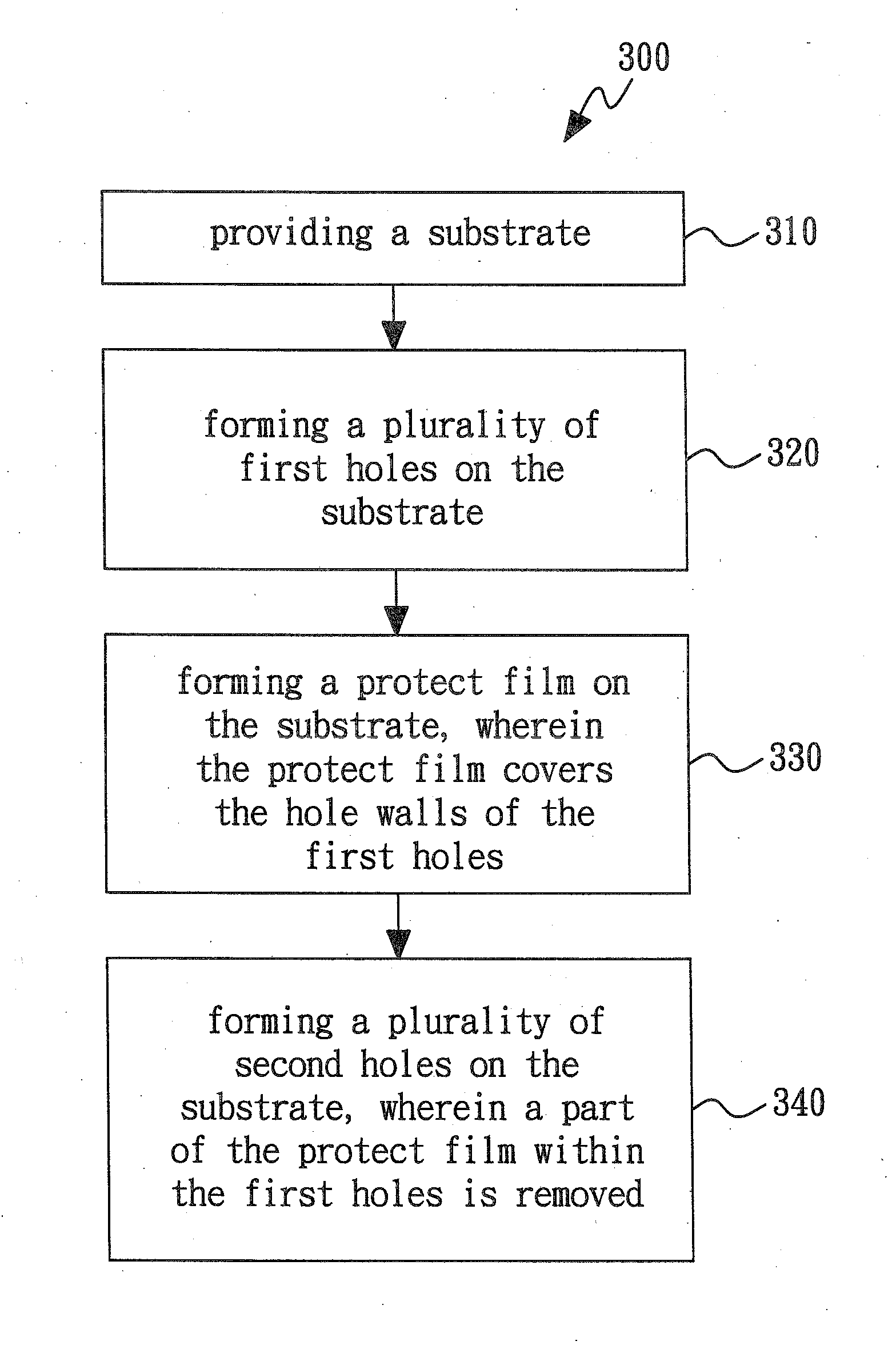
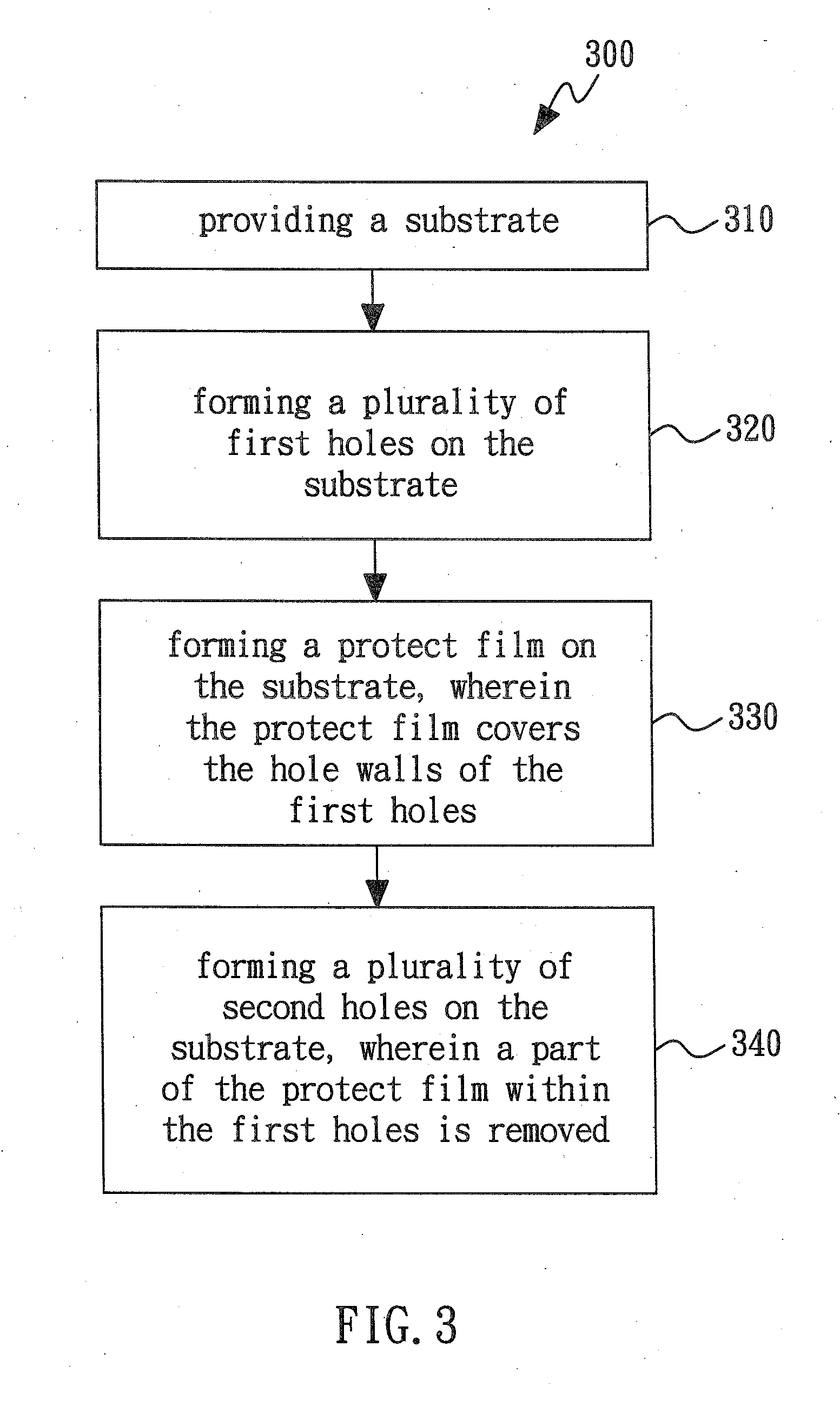
[0019]A detailed description of the present invention will be discussed in connection with the following embodiments, which are not intended to limit the scope of the present invention and which can be adapted for other applications. While the drawings are illustrated in detail, it is appreciated that the quantity of the disclosed components may be greater or less than that disclosed, except for instances expressly restricting the amount of the components.

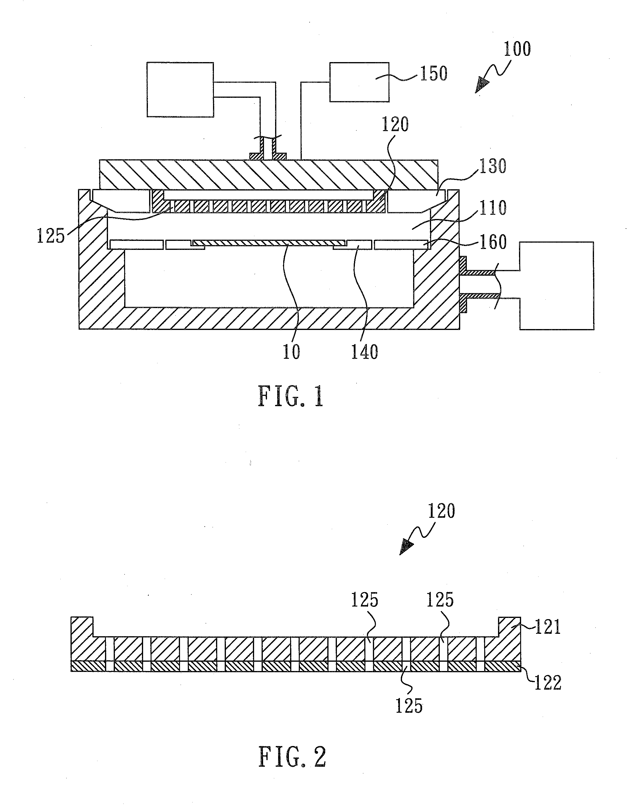
[0020]The present invention provides a showerhead for a semiconductor processing apparatus, wherein the semiconductor processing apparatus can be a plasma etching apparatus or a CVD apparatus. FIG. 1 is an explanatory view showing an overall plasma etching apparatus relating to the present invention. The plasma etching apparatus 100 comprises a process chamber 110, in which a film is formed on a surface of a wafer 10. In the process chamber 110, a showerhead 120 is disposed to face the wafer 10, and plasma is generated therein so a...


PUM

PropertyMeasurementUnit
Thicknessaaaaaaaaaa
Resistance per lengthaaaaaaaaaa
Electrical resistanceaaaaaaaaaa

Abstract

A method of making a showerhead for a semiconductor processing apparatus is disclosed. In one embodiment, the method includes providing a substrate; forming first holes in the substrate; forming a protective film on the substrate, where the protective film covers sidewalls of the first holes; and forming second holes in the substrate, where a part of the protective film within the first holes is removed. In another embodiment, the method includes providing a substrate; forming islands on the substrate; forming a protective film on the substrate, where the protective film does not cover the tops of the islands; and forming holes in the islands.

Description

BACKGROUND OF THE INVENTION[0001]1. Field of the Invention[0002]The present invention generally relates to a showerhead for a semiconductor processing apparatus, and more particularly to a showerhead for reducing contamination during semiconductor material processing.[0003]2. Description of the Prior Art[0004]In a typical plasma apparatus for etching and chemical vapor deposition (CVD) of materials on wafers, process gases are supplied into a process chamber through a showerhead, and then radio frequency (RF) waves are applied to the showerhead so as to generate a plasma of the process gases. The plasma is used to remove materials by etching or for deposition of materials on wafers. Plasma etch conditions within a process chamber tend to create a significant ion bombardment of the surfaces thereof that are exposed to the plasma.[0005]This ion bombardment, combined with plasma chemistries and / or etch byproducts, can produce significant erosion, corrosion and corrosion-erosion of the ...

Claims


Application Information

Patent Timeline
IPC IPC(8): C23C16/32C23C16/44C23C16/06
CPCC23C16/325C23C16/4404H01J37/3244C23C16/56H01J37/32091C23C16/45565
Inventor CHAO, BEN-SONCHANG, YU-FENGCHEN, YEN-SI
Owner HERMES EPITEK
Why Eureka
Try Eureka