Layout decomposition for double patterning lithography

a layout decomposition and patterning technology, applied in the field of integrated circuits and integrated circuit fabrication, can solve the problems of high output power source, high cost of conventional dpl, and many challenges of sub-wavelength lithography, and achieve the effect of reducing the total cost of layout decomposition, avoiding small jogging line-ends, and maximizing overlap at dividing points of polygons

Active Publication Date: 2011-03-31
RGT UNIV OF CALIFORNIA
View PDF4 Cites 109 Cited by
  • Summary
  • Abstract
  • Description
  • Claims
  • Application Information

AI Technical Summary

Benefits of technology

[0011]The invention provides systems and methods for layout decomposition to produce exposure layouts that can be used to perform double patterning lithography (DPL). Preferred embodiment methods of the invention are executed by a computer and provide alternate methods for layout decomposition for double patterning lithography (DPL) using coloring solutions that meet key optimization goals, which include reducing the total cost of layout decomposition, considering the abovementioned aspects that contribute to cost of prior conventional DPL techniques. Embodiments of the invention provide integer linear programming (ILP), phase conflict detection (PCD) and node election bipartization (NBD) formulations for optimization of DPL layout decomposition, with a process-aware cost function that avoids small jogging line-ends, and maximizes overlap at dividing points of polygons. The cost function can also make preferential splits at landing pads, junctions and long runs.

Problems solved by technology

Sub-wavelength lithography presents many challenges to manufacturers trying to maintain the economic scaling of semiconductors postulated by Moore's Law.
There are significant technical hurdles to implementation of EUV lithography in terms of mask-blank fabrication, high output power source, resist material, etc.
Conventional DPL increases manufacturing cost due to its complex process flows, and overlay control between the two patterning exposures becomes a critical issue.
A concern with conventional DPL is an increased manufacturing cost.
According to the International Technology Roadmap for Semiconductors, DPL requires overlay control of between 9 nm and 6 nm, which has been a major hurdle for production deployment.
A key issue in DPL from the design point of view is the decomposition of the layout for multiple exposures.
However, layout pattern configurations exist in DPL for which features within this minimum coloring spacing cannot all be assigned different colors.
The to Alternate Phase Shift Mask coloring and automatic phase shift conflict detection and resolution methods do not utilize or provide for feature splitting.
A drawback of conventional DPL pattern splitting is that it increases manufacturing cost and complexity due to (1) generation of excessive line-ends, which causes yield loss due to overlay error in double-exposure, as well as line-end shortening under defocus; and (2) resulting requirements for tight overlay control, possibly beyond currently envisioned capabilities.
Other risks include line edge (CD) errors due to overlay error, and interference mismatch between different masks.
Another key issue in DPL from the design point of view is the decomposition of the layout for multiple exposure steps.
However, there exist pattern configurations for which features within this minimum coloring spacing cannot all be assigned different colors.
The feature splitting increases manufacturing cost and complexity due to (1) generation of additional line-ends, which cause yield loss due to overlay error in double-exposure, as well as line-end shortening under defocus; and (2) resulting requirements for tight overlay control, possibly beyond currently envisioned capabilities.
Other risks include line edge (CD) errors due to overlay error, and interference mismatch between different masks.

Method used


Image

  • Layout decomposition for double patterning lithography
  • Layout decomposition for double patterning lithography
  • Layout decomposition for double patterning lithography

Examples


Embodiment Construction

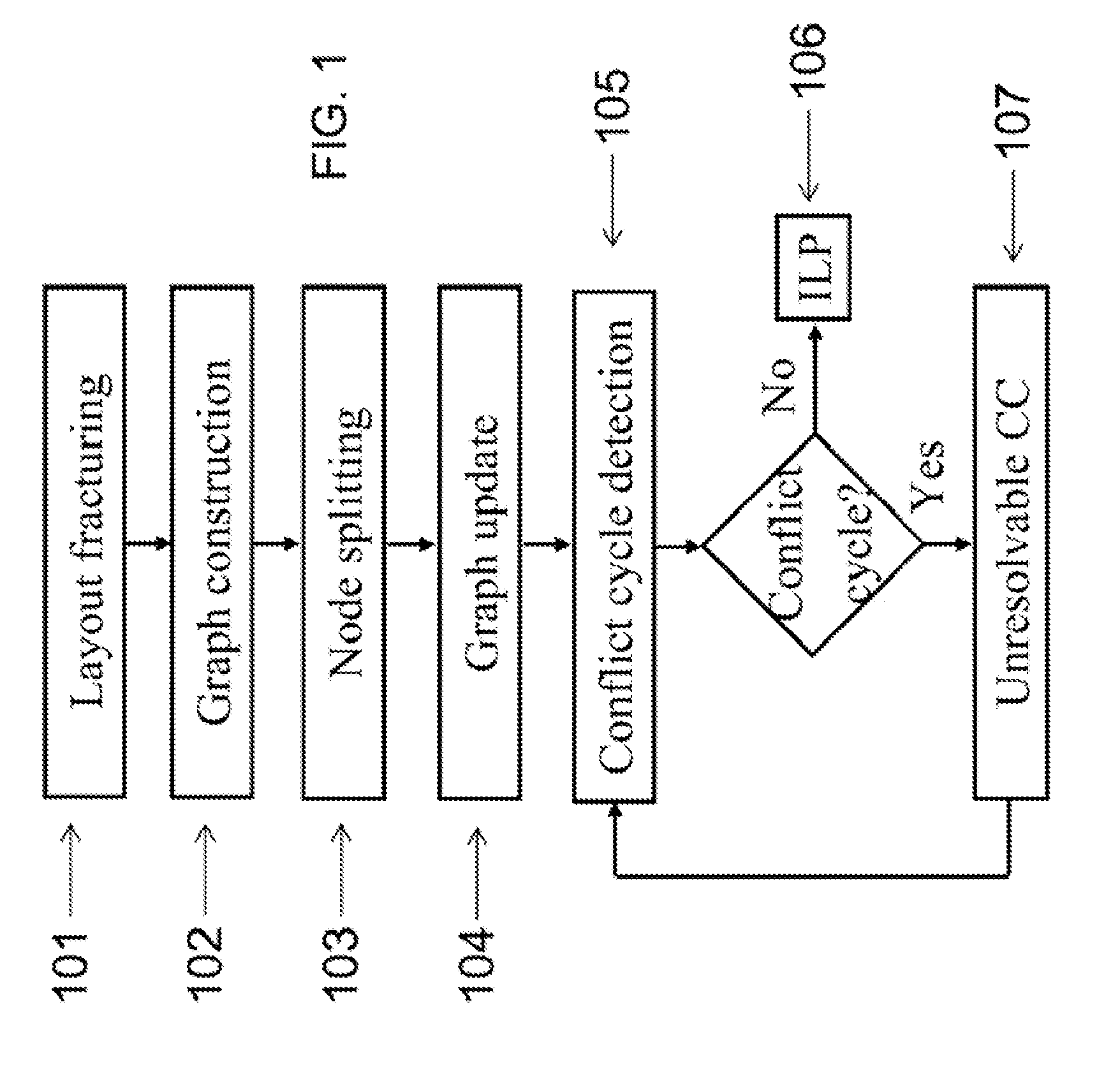
>FIG. 7 illustrates a preferred process for conflict graph generation

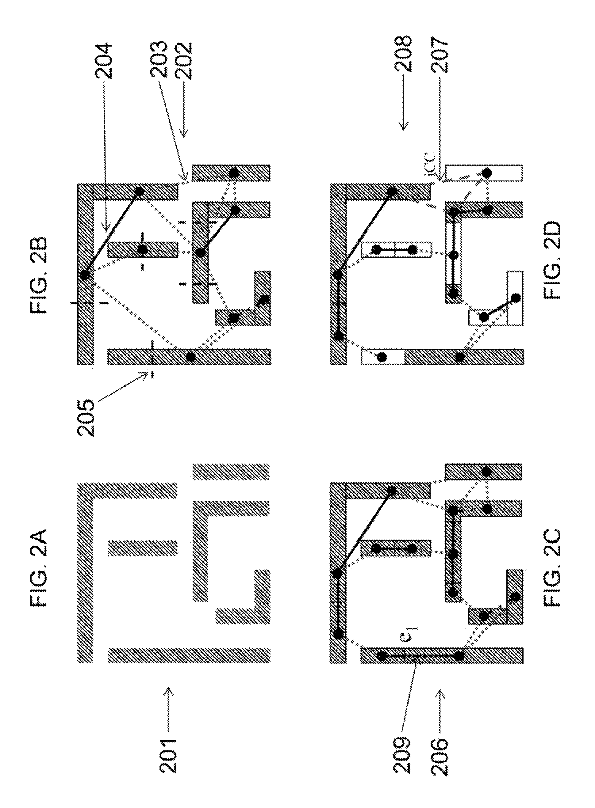
[0019]FIGS. 8A and 8B illustrate a preferred process for projecting nodes;

[0020]FIG. 9 illustrates a preferred rule-based node splitting process;

[0021]FIG. 10 shows a preferred conflict cycle detection algorithm (Algorithm 1);

[0022]FIG. 11 shows a preferred conflict cycle reporting algorithm (Algorithm 2);

[0023]FIG. 12 shows a preferred layout partitioning algorithm (Algorithm 3);

[0024]FIGS. 13A-13C show examples of a preferred conflict graph and layout coloring using preferred phase conflict detection (PCD) and node election bipartization (NBD) formulations.

DESCRIPTION OF THE PREFERRED EMBODIMENTS

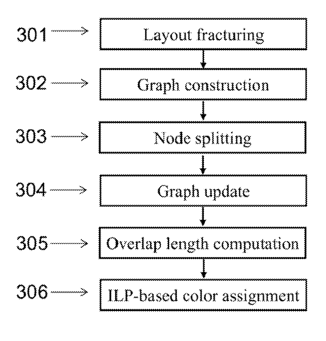
[0025]The invention provides systems and methods for layout decomposition to produce exposure layouts that can be used to perform double patterning lithography (DPL). Preferred embodiment methods of the invention are executed by a computer and provide alternate methods for layout decomposition for double patterning lithog...


PUM


Abstract

The invention provides systems and methods for layout decomposition to produce exposure layouts that can be used to perform double patterning lithography (DPL). Preferred embodiment methods of the invention are executed by a computer and provide alternate methods for layout decomposition for double patterning lithography (DPL) using integer linear programming (ILP) formulations. Embodiments of the invention meet a key optimization goals, which is to reduce the total cost of layout decomposition, considering the abovementioned aspects that contribute to cost of prior conventional DPL techniques. Embodiments of the invention provide integer linear programming (ILP), phase conflict detection (PCD) and node election bipartization (NBD) formulations for the optimization of DPL layout decomposition, with a process-aware cost function that avoids small jogging line-ends, and maximizes overlap at dividing points of polygons. The cost function can also make preferential splits at landing pads, junctions and long runs.

Description

PRIORITY CLAIM AND REFERENCE TO RELATED APPLICATION[0001]The application claims priority under 35 U.S.C. §119 from prior provisional application Ser. No. 61 / 246,613, which was filed on Sep. 29, 2009.FIELD[0002]Fields of the invention include integrated circuits and integrated circuit fabrication.BACKGROUND[0003]Lithography is an optical patterning process that patterns a material, e.g., photoresist, which is then developed to define a mask for integrated circuit fabrication processes. Reducing feature sizes to be smaller than the wavelength of light used to form the pattern in photoresist is referred to as sub-wavelength lithography. Sub-wavelength lithography presents many challenges to manufacturers trying to maintain the economic scaling of semiconductors postulated by Moore's Law. Double patterning lithography techniques are sub-wavelength techniques that are used to achieve sub 45 nm nodes with presently available manufacturing equipment. A standard single photoresist pattern b...

Claims


Application Information

Patent Timeline
Patent Type & Authority Applications(United States)
IPC IPC(8): G06F17/50
CPCG06F17/50G03F1/144G03F1/70G06F30/00
Inventor KAHNG, ANDREW B.YAO, HAILONG
Owner RGT UNIV OF CALIFORNIA
Why Eureka
Try Eureka