Silicon photodetection module

Inactive Publication Date: 2011-04-07
NAT CENT UNIV
View PDF5 Cites 4 Cited by
  • Summary
  • Abstract
  • Description
  • Claims
  • Application Information

AI Technical Summary

Benefits of technology

Another object of the present invention is to provide a silicon photodetection module, which can be made by a low-cost, non-complex process

Problems solved by technology

However, because the photocurrent photoelectrically converted from the silicon photodetector is very slight, such photocurrent cannot be applied directly, and needs to be improved.
However, this results in that the corresponding wiring pattern of these silicon photodetectors 14 becomes very complex.
Furthermore, these silicon photodetectors 14 cover a specific portion of the surface area of the positive silicon substrate 13, and this results in i

Method used


Image

  • Silicon photodetection module
  • Silicon photodetection module
  • Silicon photodetection module

Examples


Embodiment Construction

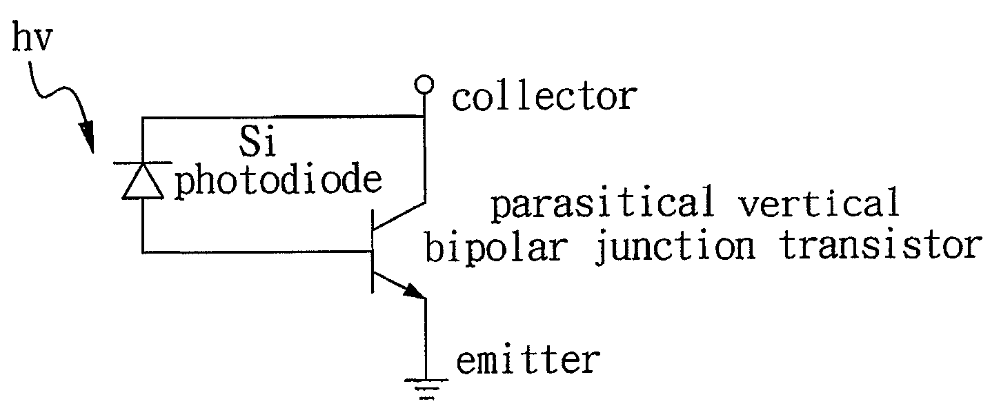
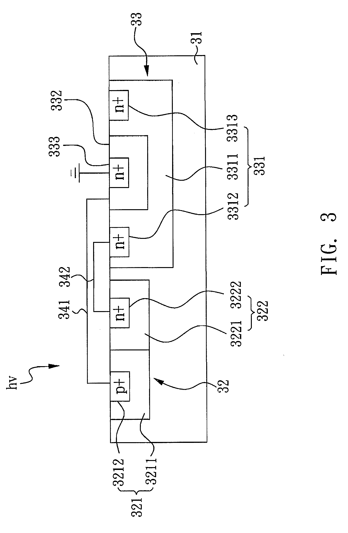
With reference to FIGS. 2 and 3, there is respectively shown an equivalent circuit and a schematic view of the silicon photodetection module in the example of the present invention. As shown in FIG. 3, in an example of the present invention, the silicon photodetection module includes: a silicon substrate 31, a silicon photodiode detection unit 32, and a parasitical vertical bipolar junction transistor amplification unit 33. The silicon photodiode detection unit 32 and the parasitical vertical bipolar junction transistor amplification unit 33 are formed on the silicon substrate 31 by a CMOS process. In addition, the silicon photodiode detection unit 32 includes a positive portion 321 and a negative portion 322, and the parasitical vertical bipolar junction transistor amplification unit 33 includes a collector 331, a base 332, and an emitter 333. Besides, the positive portion 321 of the silicon photodiode detection unit 32 is electrically connected with the base 332 of the parasitical...


PUM


Abstract

A silicon photo-detection module is disclosed, in which a silicon photodiode detection unit and a parasitical vertical bipolar junction transistor amplification unit can be simultaneously formed by a CMOS process. The silicon photo-detection module has a silicon substrate, a silicon photodiode detection unit comprising a positive portion and a negative portion, and a parasitical vertical bipolar junction transistor amplification unit comprising a collector, a base, and an emitter. The silicon photodiode detection unit and the parasitical vertical bipolar junction transistor amplification unit are formed on the silicon substrate by a CMOS process. Besides, the positive and negative portions of the silicon photodiode detection unit are electrically connected respectively with the base and the collector of the parasitical vertical bipolar junction transistor amplification unit.

Description

BACKGROUND OF THE INVENTION1. Field of the InventionThe present invention relates to a silicon photodetection module and, more particularly, to a silicon photodetection module in which a silicon photodiode detection unit and a parasitical vertical bipolar junction transistor amplification unit can be simultaneously formed by a CMOS process.2. Description of Related ArtIn a technical field of short wavelength optical communication, a silicon photodetector is commonly used as a photodetection device. However, because the photocurrent photoelectrically converted from the silicon photodetector is very slight, such photocurrent cannot be applied directly, and needs to be improved. Therefore, several solutions of the abovementioned problems have been reported. One of these solutions is to arrange a plurality of silicon photodetectors in an array so as to form a silicon photodetector array as shown in FIG. 1. The silicon photodetector array is made by the following procedures. First, using...

Claims


Application Information

Patent Timeline
IPC IPC(8): H01L31/102H03F3/08
CPCH01L31/103H03F3/08H01L31/1105
Inventor HSIN, YUE-MINGCHOU, FANG-PINGCHEN, GUAN-YU
Owner NAT CENT UNIV
Why Eureka
Try Eureka