Dram cell with double-gate fin-fet, dram cell array and fabrication method thereof

a technology of dram cell and fin-fet, which is applied in the field of dram cell array and fabrication method thereof, and dynamic random access memory (dram) cell array, which can solve the problems of increasing leakage current, increasing the difficulty of retaining the current driver capability of the transistor, and increasing the complexity of process engineering of vertically embodied transistors

Active Publication Date: 2011-04-07
NAN YA TECH
View PDF3 Cites 59 Cited by
  • Summary
  • Abstract
  • Description
  • Claims
  • Application Information

AI Technical Summary

Benefits of technology

[0011]It is therefore the primary objective to provide an improved DRAM cell structure, DRAM cell array and a fabrication method thereof in order to solve the above-mentioned prior art problems.

Problems solved by technology

As the areas of the memory cells become smaller and smaller on account of increasing miniaturization, retaining the current driver capability of the transistor poses an increasing problem.
However, there is the problem of increased leakage currents when the gate oxide thickness is reduced or the doping concentrations are higher.
However, vertically embodied transistors are very complicated in terms of process engineering and can be fabricated only with difficulty, in particular with regard to the connection technique of the source / drain regions and of the gate electrodes of the transistor.
Further, during the operations of switching the transistor on and off, the semiconductor substrate is also concomitantly charged at the same time, and the so-called floating body effect occurs, as a result of which the switching speed of the transistor is greatly impaired.
However, the conventional DRAM device with double gate fin-FET have drawbacks including complexity of the manufacturing processes, floating body effect and insufficient source / drain contact area that leads to high contact / junction resistance and reduced performance.

Method used


Image

  • Dram cell with double-gate fin-fet, dram cell array and fabrication method thereof
  • Dram cell with double-gate fin-fet, dram cell array and fabrication method thereof
  • Dram cell with double-gate fin-fet, dram cell array and fabrication method thereof

Examples


Embodiment Construction

[0037]In the following detailed description, reference is made to the accompanying drawings which form a part hereof, and in which is shown by way of illustration specific embodiments in which the invention may be practiced. These embodiments are described in sufficient detail to enable those skilled in the art to practice the invention, and it is to be understood that other embodiments may be utilized and that structural, logical and electrical changes may be made without departing from the spirit and scope of the present invention. The following detailed description is, therefore, not to be taken in a limiting sense, and the scope of the present invention is defined by the appended claims.

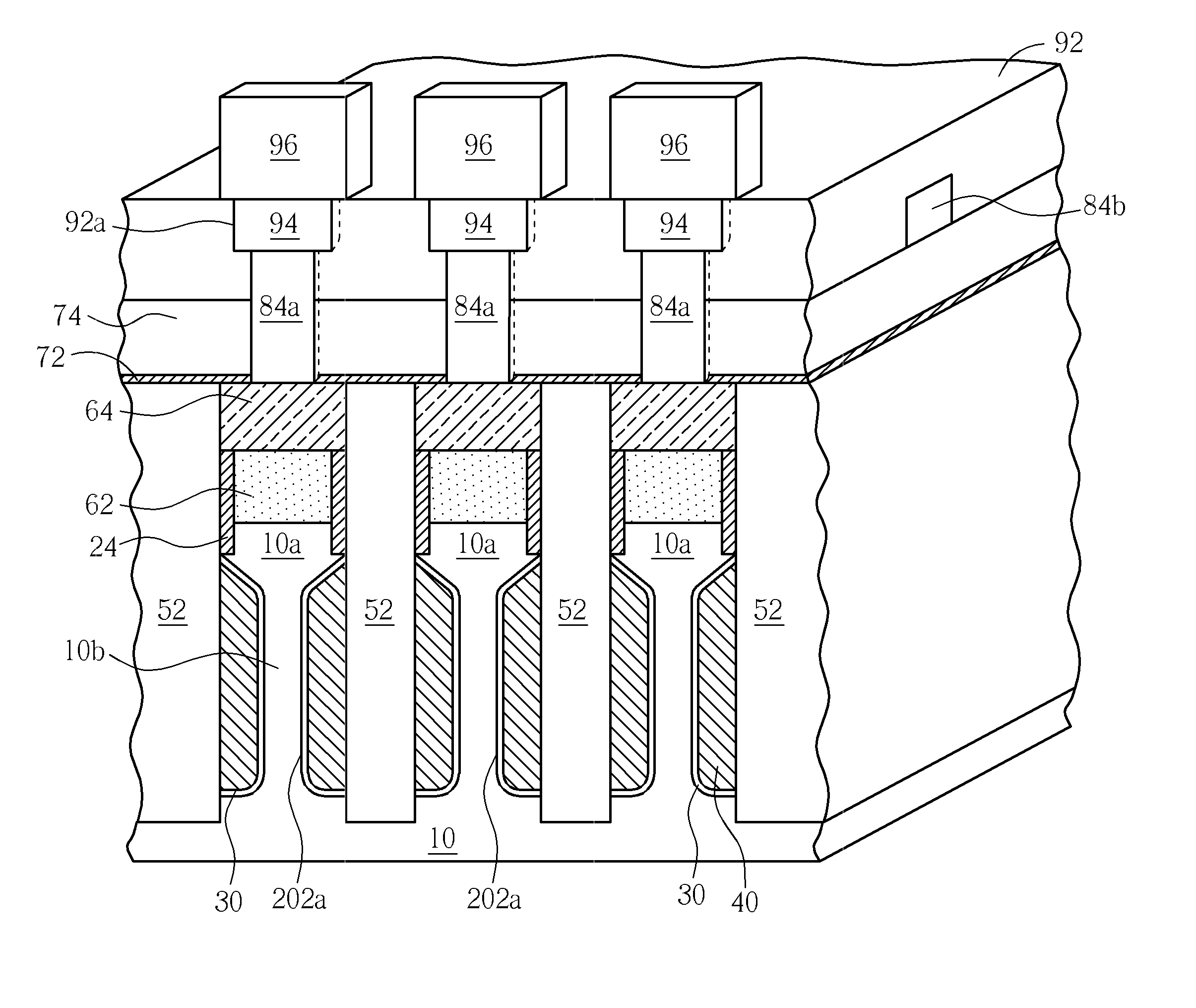
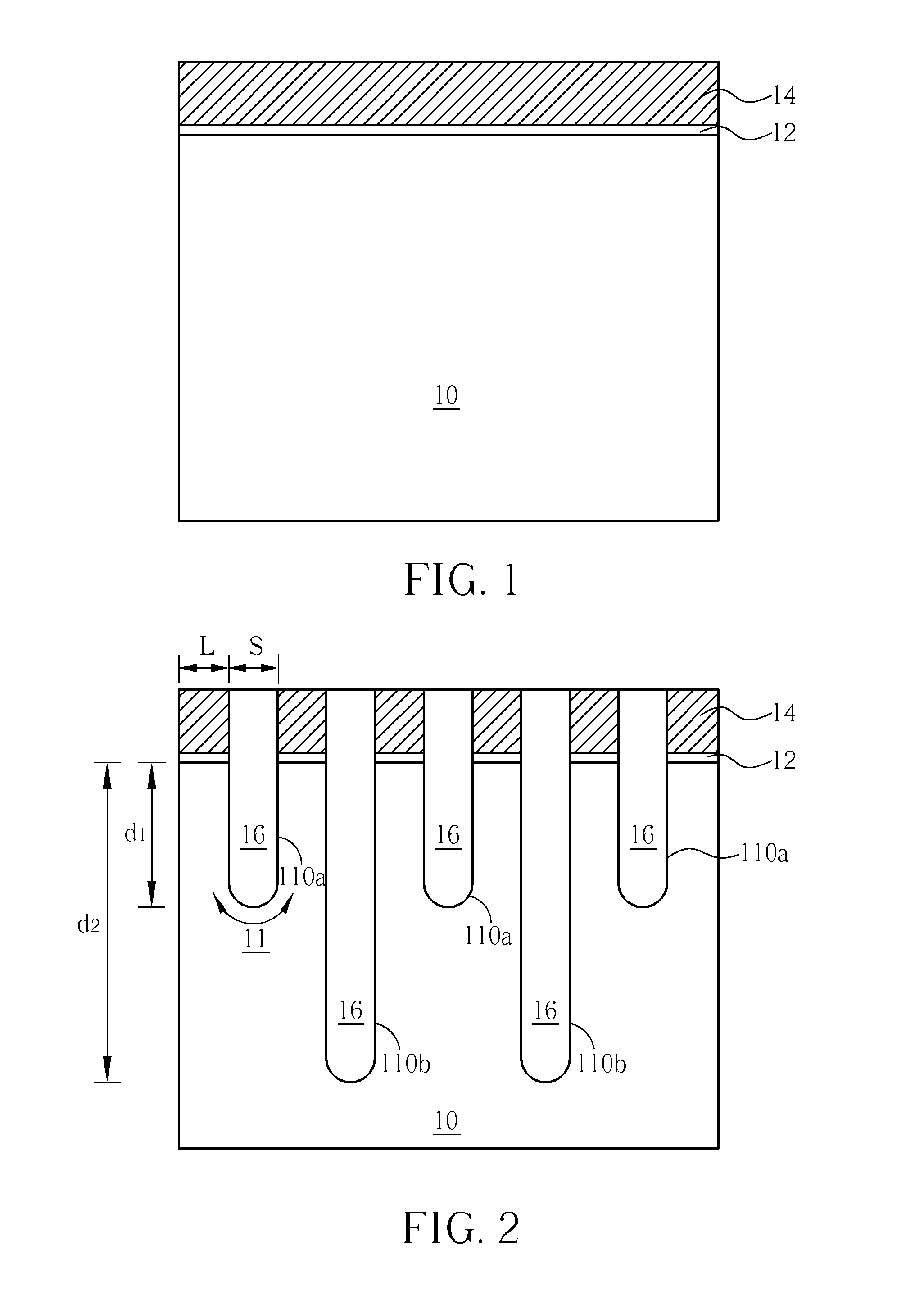
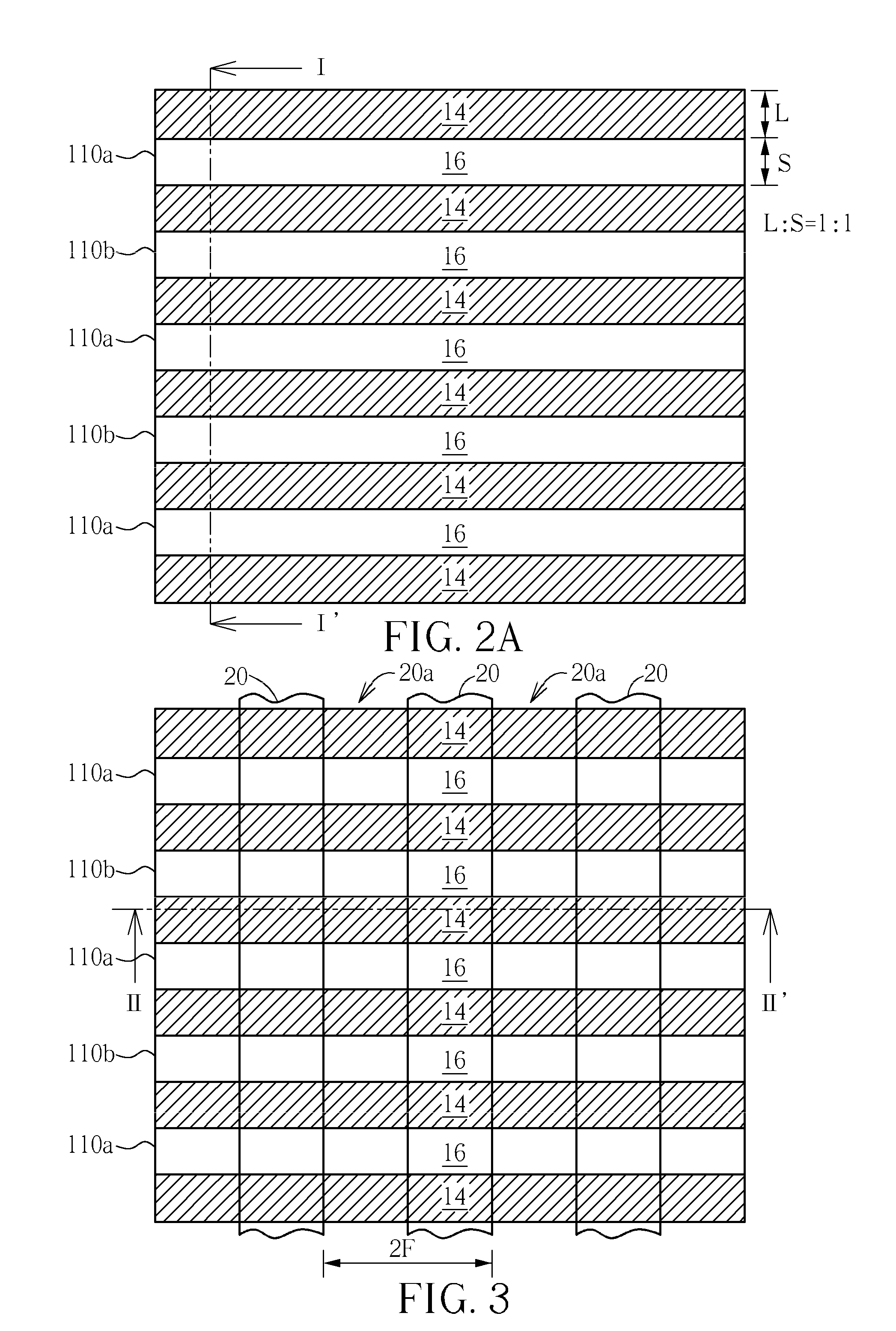
[0038]Referring initially to FIG. 1, a semiconductor substrate 10 is provided. On the main surface of the semiconductor substrate 10, a pad oxide layer 12 is formed by methods known in the art such as oxidation or deposition methods. A pad nitride layer 14 is then deposited on the pad oxide layer...


PUM


Abstract

A transistor structure includes a semiconductor substrate having a top surface and sidewalls extending downward from the top surface, wherein each of the sidewall comprises a vertical upper sidewall surface and a lower sidewall recess laterally etched into the semiconductor substrate. A trench fill dielectric region is inlaid into the top surface of the semiconductor substrate. Two source / drain regions are formed into the top surface of the semiconductor substrate and are sandwiched about the trench fill region. A buried gate electrode is embedded in the lower sidewall recess. A gate dielectric layer is formed on surface of the lower sidewall recess between the semiconductor substrate and the buried gate electrode.

Description

BACKGROUND OF THE INVENTION[0001]1. Field of the Invention[0002]The present invention relates generally to semiconductor technologies. More particularly, the present invention relates to a dynamic random access memory (DRAM) cell and array with an embedded double-gate fin-FET, and a method for fabricating such DRAM cell structure.[0003]2. Description of the Prior Art[0004]Currently used dynamic random access memory (DRAM) devices comprise memory cells with one transistor and one storage capacitor in series. In order to obtain a sufficiently large read signal of the DRAM memory cell, the storage capacitor has to provide a sufficient storage capacitance. On account of the limited memory cell area, storage capacitors which utilize the third dimension are therefore used. One embodiment of a three-dimensional storage capacitor is the so-called stacked capacitor, which is arranged in a manner laterally adjoining a transistor, preferably essentially above the transistor, the inner capacito...

Claims


Application Information

Patent Timeline
Patent Type & Authority Applications(United States)
IPC IPC(8): H01L27/108H01L21/8242
CPCH01L27/10826H01L27/10891H01L27/10876H10B12/36H10B12/053H10B12/488
Inventor LIN, SHIAN-JYH
Owner NAN YA TECH
Why Eureka
Try Eureka