
Capacitive proximity device and electronic device comprising the capacitive proximity device

Active Publication Date: 2011-04-14
KONINKLIJKE PHILIPS ELECTRONICS NV
View PDF12 Cites 25 Cited by
  • Summary
  • Abstract
  • Description
  • Claims
  • Application Information

AI Technical Summary

Benefits of technology

It is an object of the invention to provide a capacitive proximity device having improved reliability.
The capacitive proximity device, for example, generates a specific output-signal level referring to a situation in which no person is in the neighborhood of the display device. This signal level may be indicated as “infinity-signal level” indicating that this is the maximum signal level when nobody is in the neighborhood of the display device. When the output-signal level decreases the object or person approaches the display device. The capacitive proximity device according to the invention may, for example, be configured to switch off the energy reduction mode when the output-signal level is below the first proximity reference level. The display device, for example, switches on and displays the current information to the user. The capacitive proximity device according to the invention may also have a second proximity reference level which is substantially above the “infinity-signal level”. This second proximity reference level is used to indicate a situation in which the object or person is very close to the capacitive proximity device, for example, 20 millimeter or less. When the person or object is very close to the capacitive proximity device, the person or object starts to be part of the capacitive proximity device and increases the capacitive coupling between the emission electrode and the receiver electrode considerably. In such a situation, the output-signal typically substantially exceeds the “infinity-signal level”. This may, for example, occur when a person wants to adapt settings of a display device and has to operate switches at the outer surface of the display device. When such high signal is detected, the display device must remain switched on and should not start an energy reduction mode to ensure that the user may, for example, see the adaptations he is performing. To avoid the display device to switch to the energy reduction mode during the relatively quick change from the output-signal level below the first proximity reference level to the output-signal level above the second proximity reference level, a short delay time may be incorporated before the display device switches to the energy reduction mode.

Problems solved by technology

A disadvantage of active infrared and ultrasound sensors are their dependency with respect to the material of the object.
Clothing may absorb the transmitted energy too much thereby reducing the detection range or give false distance readings.
Also the field of view is often relatively narrow resulting in a sensitive area only in the direct centre line in front of the display device.
This may be solved by using more sensors directing in different directions—however this results in a relatively expensive solution.
Passive infrared sensors will not react on stationary (warm) objects, so when a person doesn't move enough in front of the monitor, the energy reduction mode will be activated which again may be an unwanted situation.
A drawback of the known capacitive sensor is that the registration of a person by the known capacitive sensor is not reliable enough.

Method used


Image

  • Capacitive proximity device and electronic device comprising the capacitive proximity device
  • Capacitive proximity device and electronic device comprising the capacitive proximity device
  • Capacitive proximity device and electronic device comprising the capacitive proximity device

Examples


Embodiment Construction

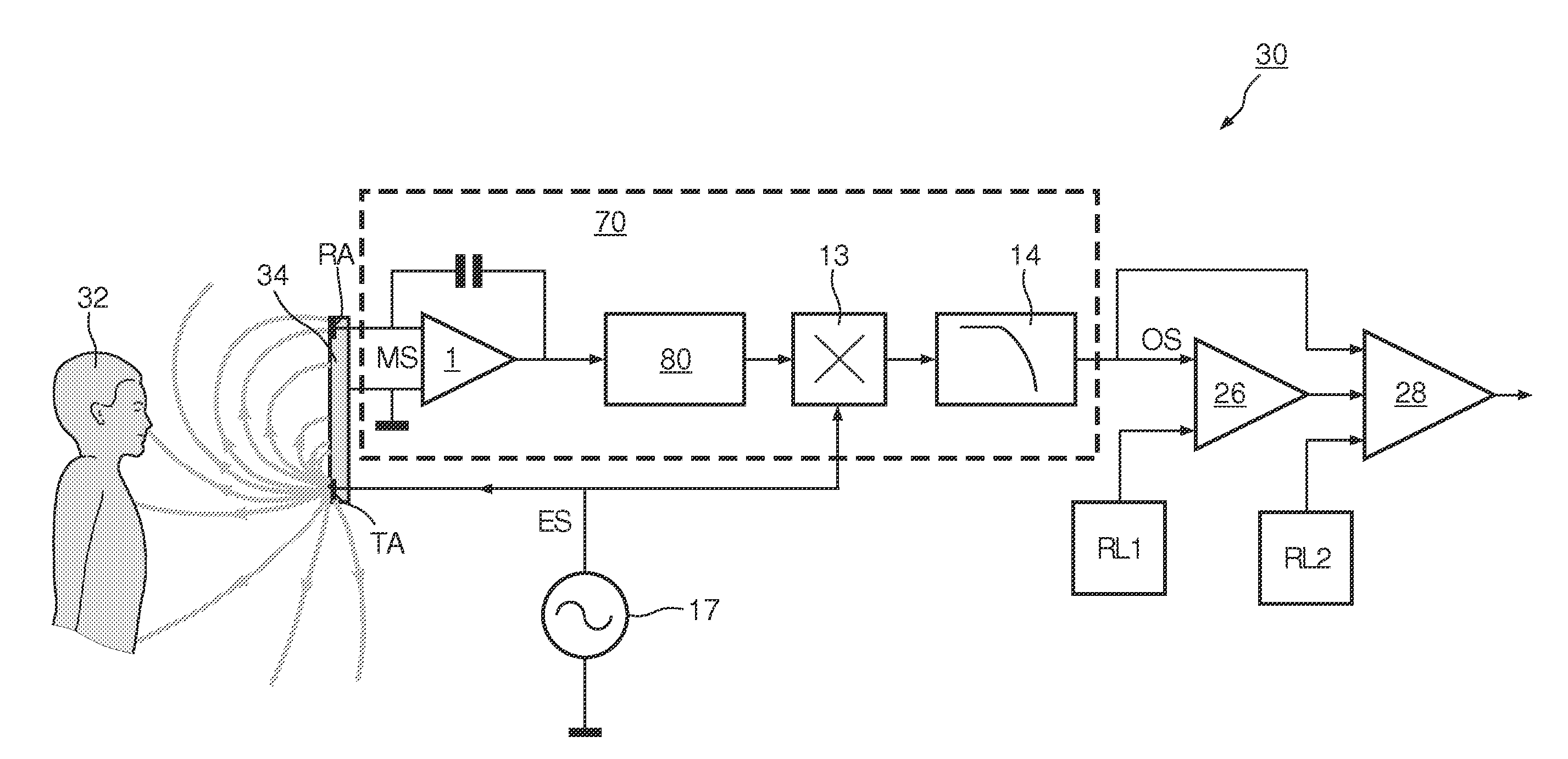
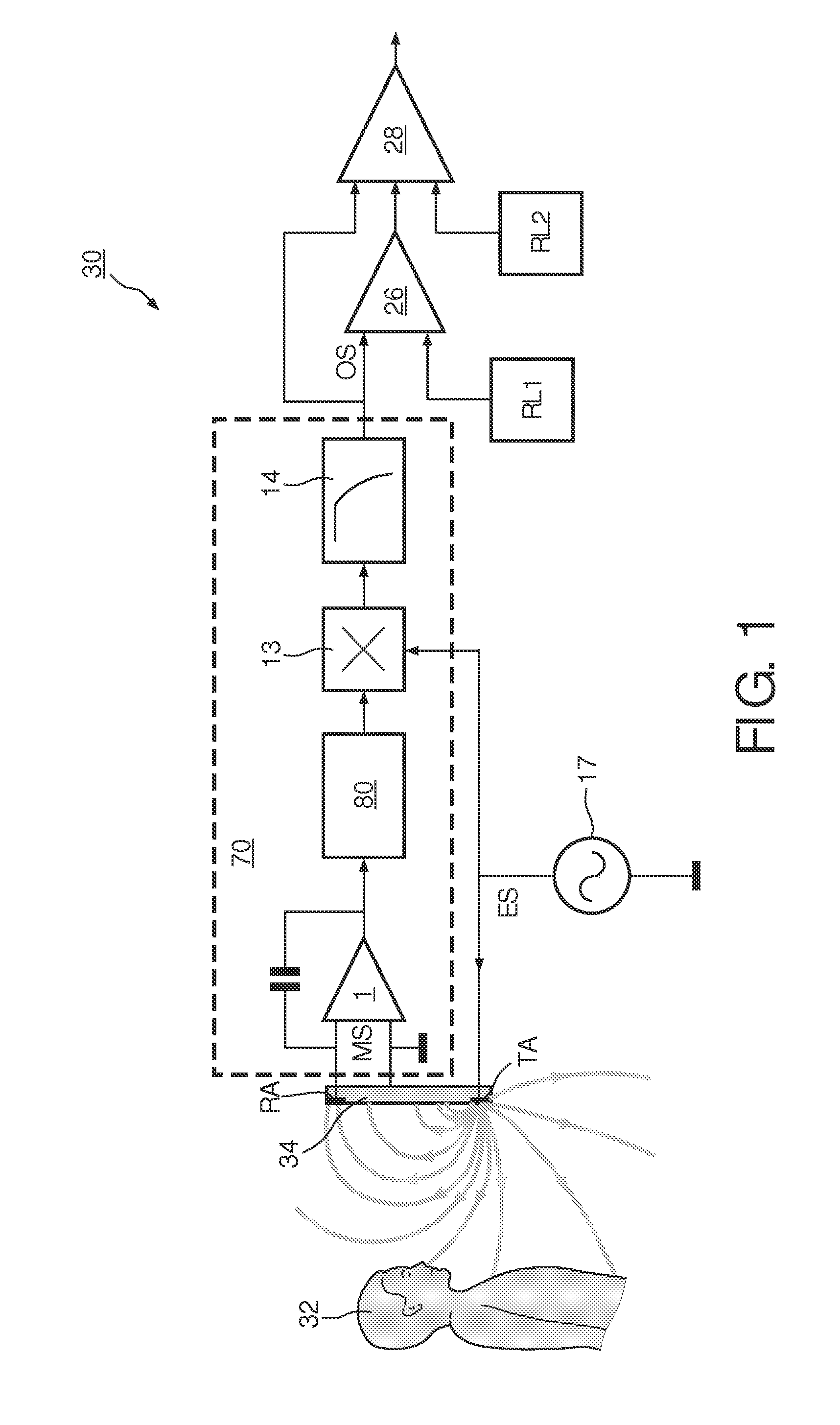
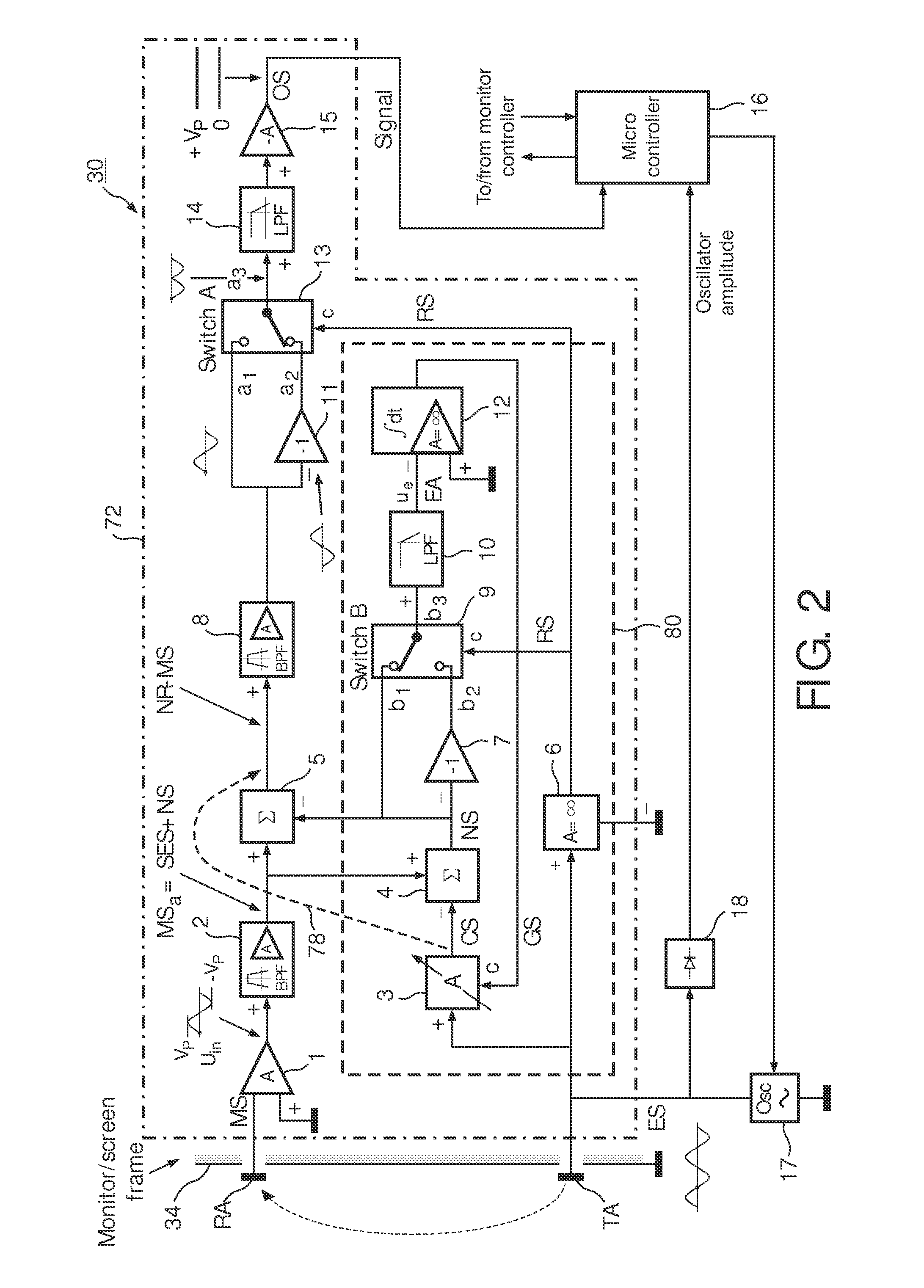
FIG. 1 shows a schematic representation of a capacitive proximity device 30 according to the invention. The capacitive device 30 is arranged at an electronic device, for example, a display device 34 and typically at the rim of the display device 34. The capacitive proximity device 30 comprises an emission electrode TA, in the example shown in FIG. 1 arranged at the bottom-rim of the display device 34, and a receiver electrode RA, in the example shown in FIG. 1 the receiver electrode RA is arranged at the top-rim of the display device 34. An oscillator 17 is connected to the emission electrode TA and generates an emission signal ES which is emitted via the emission electrode TA to generate an alternating electric field (indicated in FIG. 1 with the curved lines comprising an arrow which originate from the emission electrode TA. The capacitive proximity device 30 further comprises a sensing circuit 70 connected to the receiver electrode RA and arranged for detecting and amplifying the...


PUM


Abstract

The invention relates to a capacitive proximity device (30, 40, 50, 60) for sensing a presence and / or absence of an object (32) in the proximity of an electronic device (34). The capacitive proximity device (30, 40, 50, 60) comprises: an emission electrode (TA) capacitively coupled to a receiver electrode ( ), an oscillator (17) for generating an emission-signal (ES) being an alternating electric field ( ) between the emission electrode (TA) and the receiving electrode ( ), and a sensing circuit (70, 72, 74, 76, 78) connected to the receiving electrode ( ). The sensing circuit receives a measured-signal (MS) from the receiver electrode ( ), and comprising a first synchronous detection circuit ( ) together with a low-pass filter (14) for generating an output-signal (OS) being proportional to a distance between the object and the electronic device. The sensing circuit further comprising noise-suppression means for reducing noise from the measured-signal (MS) before entering the first synchronous detection circuit. The inventors have found that additional noise-suppression techniques are required when applying the known capacitive sensors in a electronic device.

Description

FIELD OF THE INVENTIONThe invention relates to a capacitive proximity device of an electronic device. The invention further relates to an electronic device comprising the capacitive proximity device, and to a sensing circuit for the capacitive proximity device.BACKGROUND OF THE INVENTION:Reduction of energy consumption in display devices when the display device is not used, is known, for example, in monitors for personal computers and / or laptops. In such a system, the activity of a user is measured, for example, by detecting key-strokes of the user or mouse-movements of the user. In case the user has not stroke a key for some predetermined time, or has not moved the mouse of the computer and / or laptop for some predetermined time, the display device enters a so called energy reduction mode which may also be called a “sleep mode” in which the display device switches off, or in which the backlight of the display device switches off. However, often the display device switches to the ene...

Claims


Application Information

Patent Timeline
IPC IPC(8): G01R27/26
CPCH03K17/955G01R27/2605G01N27/221H03K2217/960775H03K17/96H03K2217/96077
Inventor ASJES, RONALD JANROMMERS, ADRIANUS PETRUS JOHANNA MARIAVERSPAGET, HENRICUS ANTONIUSPRESURA, CRISTIANBLOM, ANTONIUS HERMANUS MARIA
Owner KONINKLIJKE PHILIPS ELECTRONICS NV
Learn More