Method for Fracturing a Pattern for Writing with a Shaped Charged Particle Beam Writing System Using Dragged Shots

a writing system and shaped beam technology, applied in the field of lithography, can solve the problems of expensive computation time, difficult to accurately translate the physical design to the actual circuit pattern developed on the resist layer, and laborious task of adding opc features,

Inactive Publication Date: 2011-04-21
D2S
View PDF9 Cites 20 Cited by
  • Summary
  • Abstract
  • Description
  • Claims
  • Application Information

AI Technical Summary

Benefits of technology

[0013]A method and system for fracturing or mask data preparation or proximity effect correction is disclosed, wherein a shot determined for a shaped charged particle beam writer system comprises dragging the charged particle beam across a surface during the shot, so as to form a complex pattern in a single, extended shot. The dragging may be done with either variable shaped beam (VSB) or character projection (CP) shots. Methods for specifying in the shot data the path for the dragged shot are also disclosed. Other embodiments include using dragged shots with partial projection, varying the dragging velocity during a shot, and combining dragged shots with conventional shots.

Problems solved by technology

An example of an end-use limitation is defining the geometry of a transistor in a way in which it cannot sufficiently operate at the required supply voltage.
The design rule limitations reflect, among other things, the smallest dimensions that can be reliably fabricated.
As the critical dimensions of the circuit pattern become smaller and approach the resolution value of the exposure tool, the accurate transcription of the physical design to the actual circuit pattern developed on the resist layer becomes difficult.
Adding OPC features is a very laborious task, requires costly computation time, and results in more expensive reticles.
Not only are OPC patterns complex, but since optical proximity effects are long range compared to minimum line and space dimensions, the correct OPC patterns in a given location depend significantly on what other geometry is in the neighborhood.
There are numerous manufacturing factors that also cause variations, but the OPC component of that overall error is often in the range listed.
Since curvilinear patterns are difficult and expensive to form on a reticle using conventional techniques, rectilinear approximations of the curvilinear patterns may be used.
The cost of shaped beam charged particle beam lithography is directly related to the time required to expose a pattern on a surface, such as a reticle or wafer.
For the most complex integrated circuit designs, forming the set of layer patterns on a set of reticles is a costly and time-consuming process.

Method used


Image

  • Method for Fracturing a Pattern for Writing with a Shaped Charged Particle Beam Writing System Using Dragged Shots
  • Method for Fracturing a Pattern for Writing with a Shaped Charged Particle Beam Writing System Using Dragged Shots
  • Method for Fracturing a Pattern for Writing with a Shaped Charged Particle Beam Writing System Using Dragged Shots

Examples


Embodiment Construction

[0034]The improvements and advantages of the present disclosure can be accomplished by use of a shaped beam charged particle beam writer system in which the beam can be moved or dragged during a shot over a specified path, and by creating and using a shot list which contains information with which to control the charged particle beam writer system in making the dragged shot.

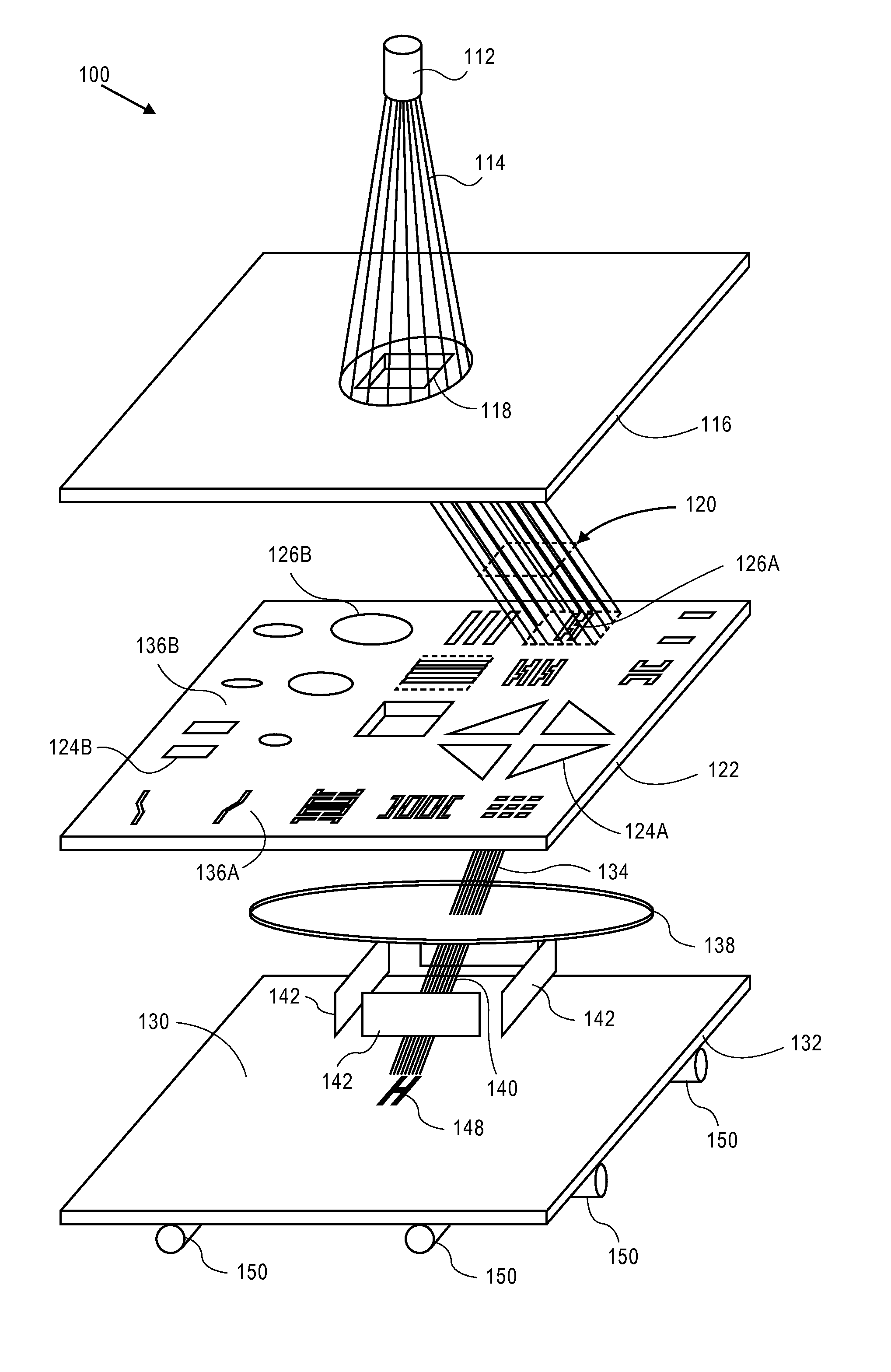
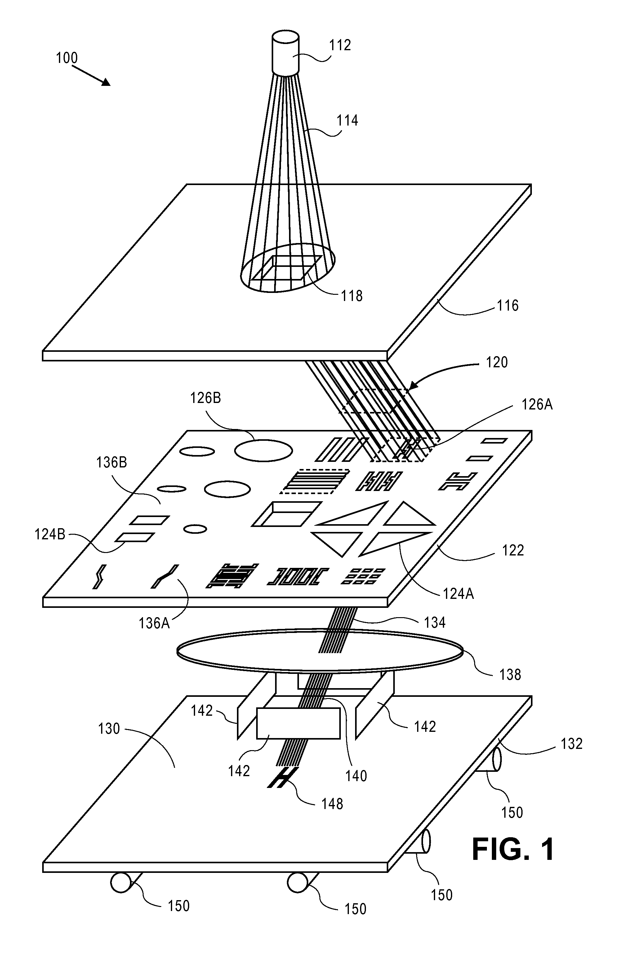
[0035]Referring now to the drawings, wherein like numbers refer to like items, FIG. 1 illustrates an embodiment of a conventional lithography system 100, such as a charged particle beam writer system, in this case an electron beam writer system, that employs character projection to manufacture a surface 130. The electron beam writer system 100 has an electron beam source 112 that projects an electron beam 114 toward an aperture plate 116. The plate 116 has an aperture 118 formed therein which allows the electron beam 114 to pass. Once the electron beam 114 passes through the aperture 118 it is directed or deflect...


PUM


Abstract

In the field of semiconductor production using shaped charged particle beam lithography, a method and system for fracturing or mask data preparation or proximity effect correction is disclosed, wherein a shot determined for a shaped charged particle beam writer system comprises dragging the charged particle beam across a surface during the shot, so as to form a complex pattern in a single, extended shot. The dragging may be done with either variable shaped beam (VSB) or character projection (CP) shots. Methods for specifying in the shot data the path for the dragged shot are also disclosed. Other embodiments include using dragged shots with partial projection, varying the dragging velocity during a shot, and combining dragged shots with conventional shots. A method and system for creating glyphs which contain dragged shots is also disclosed.

Description

RELATED APPLICATIONS[0001]This application is related to Komagata, U.S. patent application Ser. No. ______ entitled “Method and System for Manufacturing a Surface By Dragging Characters Using Shaped Charged Particle Beam Lithography” (Attorney Docket No. D2SiP024P), filed on even date herewith and which is hereby incorporated by reference for all purposes.BACKGROUND OF THE DISCLOSURE[0002]The present disclosure is related to lithography, and more particularly to the design of a shaped beam charged particle beam writer system and methods for using the shaped beam charged particle beam writer system to manufacture a surface which may be a reticle, a wafer, or any other surface.[0003]In the production or manufacturing of semiconductor devices, such as integrated circuits, optical lithography may be used to fabricate the semiconductor devices. Optical lithography is a printing process in which a lithographic mask or photomask manufactured from a reticle is used to transfer patterns to a...

Claims


Application Information

Patent Timeline
Patent Type & Authority Applications(United States)
IPC IPC(8): G21K5/10H01J37/08
CPCB82Y10/00B82Y40/00H01J37/3174G03F7/2063G03F1/78Y10S430/143
Inventor FUJIMURA, AKIRAZABLE, HAROLD ROBERTTUCKER, MICHAEL
Owner D2S
Why Eureka
Try Eureka