

Semiconductor device design method
a technology of semiconductor devices and design methods, applied in the direction of cad circuit design, program control, instruments, etc., can solve the problems of increasing the overall layout processing time, and uneven amount of each processing data, so as to achieve the effect of optimizing the layout design
- Summary
- Abstract
- Description
- Claims
- Application Information
AI Technical Summary
Benefits of technology
Problems solved by technology
Method used
Image

Examples
first embodiment
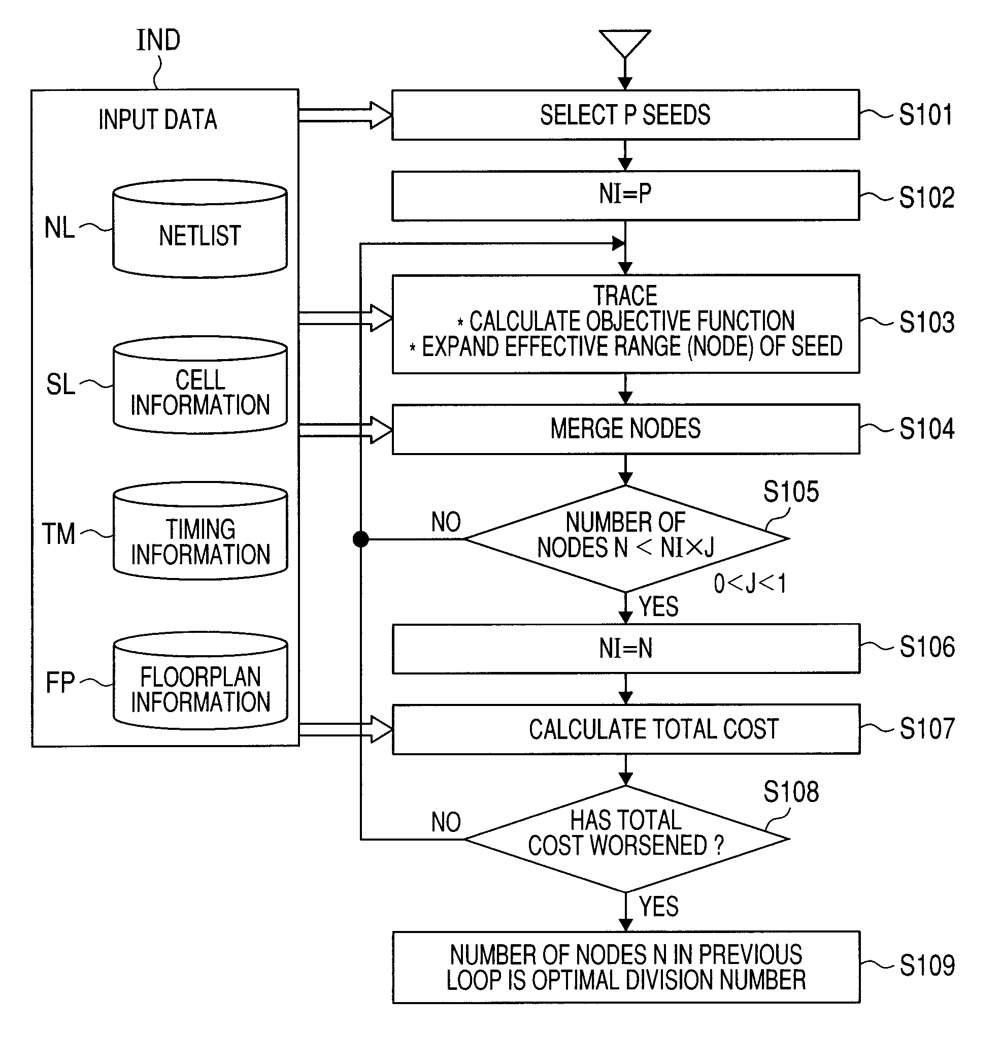
[0056]FIG. 1 is a flowchart showing an example of processing in a semiconductor device design method according to the first embodiment of the invention. The semiconductor device design method shown in FIG. 1 is implemented when a computer system executes programs in response to input data IND stored in a storage unit such as a hard disk. The input data IND contains a netlist NL, cell information SL about each cell contained in the netlist, timing information TM, and floorplan information FP in some cases.
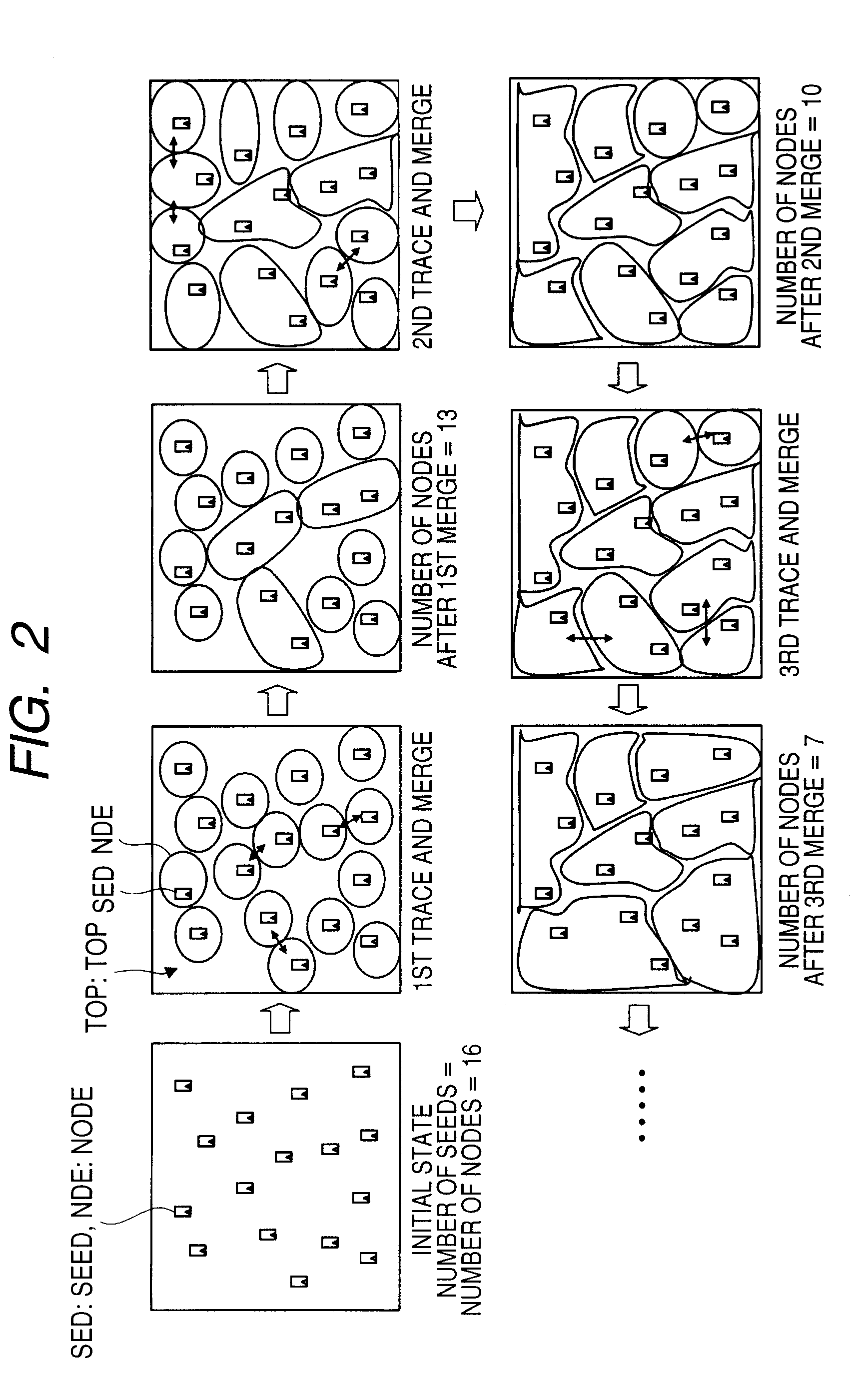
[0057]In FIG. 1, first, the computer system refers to the netlist NL and selects P seeds therefrom (S101). Each seed is a flip-flop. After setting a reference value NI=P (S102), the computer system performs a trace (S103). In the trace, the computer system refers to the netlist NL and takes in preceding or subsequent flip-flops coupled to each seed as an origin, thereby expanding the effective range (referred to as “node”) of each seed in stages and in parallel. At this time, the co...
second embodiment
[0097]In the second embodiment, description will be made as to the application of the design method according to the first embodiment to parallel automatic layout using a plurality of computer systems having different processing capabilities. In the first embodiment, division is performed so as to equalize the respective objective function values (including layout processing time) of the nodes. However, in the case where distributed processing hardware devices have different specs, the processing time may be shortened if the respective objective function values of the nodes have a predetermined ratio according to the different specs. Accordingly, in a semiconductor device design method according to the second embodiment, appropriate division is performed in consideration of the specs (CPU, memory) of distributed processing hardware devices, and each processing is assigned to the respective hardware device.
[0098]For example, the hardware specs of the computer systems for performing a...
third embodiment
[0101]In the third embodiment, the design method of FIG. 1 according to the first embodiment will be described in greater detail. FIG. 20 is a flowchart showing an example of processing in a semiconductor device design method according to the third embodiment of the invention. In FIG. 20, first, the computer system selects M seeds in the same way as in S101 of FIG. 1 (S2001), and substitutes M for the number of remaining seeds (the number of not-yet-subgraphed seeds) X, 0 for the number of subgraphs S, and X+S for the number of nodes N as initial conditions (S2002). Then, after setting a reference value XI=M (S2003), the computer system performs a trace.
[0102]In the trace, the computer system repeats the loop processing of trace graph generation (S2004), objective-function calculation (S2005), and node expansion (S2006) until the number of remaining seeds X≦XI×K (S2007). K is an arbitrary value between 0 and 1 (02008).
[0103]Then, after setting a reference value NI=X+S (S2009), the c...
PUM
 Abstract
Description
Claims
Application Information