Chip filter and the related supplementary tool

a chip filter and supplementary tool technology, applied in the direction of sustainable manufacturing/processing, coupling device connection, final product manufacturing, etc., can solve the problems of affecting the normal functioning of the local area network, wasting time and labor, and affecting the signal transmission, so as to reduce the material consumption of the connection terminal and facilitate the installation of the connection terminal. , the effect of quick and accurate bonding

Inactive Publication Date: 2011-04-28
U D ELECTRONIC CORP
View PDF16 Cites 37 Cited by
  • Summary
  • Abstract
  • Description
  • Claims
  • Application Information

AI Technical Summary

Benefits of technology

[0015]The present invention has been accomplished under the circumstances in view. It is one object of the present invention to provide a chip filter and supplementary tool, which facilitates bonding the lead wires of filter elements of the chip filter to the respective connection terminals, saving much labor and time and improving the productivity.
[0017]Further, the base portion of each connection terminal of the chip filter has a width greater than the width of the wire grooves of the insulative holder base. Further, the bonding tip of each connection terminal of the chip filter extends outwardly from an outer end of the associating base portion outside the associating sidewall of the insulative holder base. Further, each connection terminal of the chip filter has an opening defined in a front side relative to the base portion at one side of the bonding tip thereof and aimed at one wire groove, facilitating positioning of the lead wires for quick and accurate bonding.
[0018]Further, the base portions of the connection terminals of the chip filter are positioned in the sidewalls of the insulative holder base during molding of the insulation holder base, and each connection terminal has an interference block extended upwardly from one end of the associating base portion opposite to the associating bonding tip and embedded in one sidewall of the insulative holder base. Thus, the material consumption of the connection terminals is minimized, and the installation of the connection terminals is simplified.
[0019]Further, subject to the application of the supplementary tool, the lead wires of the filter elements can be automatically set in the respective wire grooves of the insulative holder base and the respective locating grooves and secured to narrow crevices in tool base of the supplementary tool by a mechanical arm for quick bonding to the soldering surfaces of the base portions of the connection terminals by an automatic soldering machine, simplifying the fabrication and increasing the productivity.

Problems solved by technology

Further, during signal transmission of a network interface component, for example, RJ-45 Connector, it may cause an electromagnetic interference with surrounding electronic components or circuits, or the surrounding noises may interfere with the transmission of signal through the RJ-45 connector, resulting a signal transmission error.
The electromagnetic interference may disturb surrounding wireless signal transmission, affecting normal functioning of the local area network.
1. Winding the lead wires C1 of the filter elements C round the top pins B2 of the metal terminals B wastes much time and labor, complicating the operation and increasing the cost.
2. Because the metal terminals B extend through the height of the electrically insulative housing A, they must have a certain length, increasing the material cost.
3. Because the top pins B2 of the metal terminals B protrude over the topmost edge of the electrically insulative housing A for the fastening of the lead wires C1 of the filter elements C, the top cover D is necessary for protection. The use of the top cover D complicates the fabrication and cost of the signal filter module.
It takes much labor and time to set the wires G1 and the conductors H in position for bonding, increasing the cost and lowering the productivity.

Method used


Image

  • Chip filter and the related supplementary tool
  • Chip filter and the related supplementary tool
  • Chip filter and the related supplementary tool

Examples


first embodiment

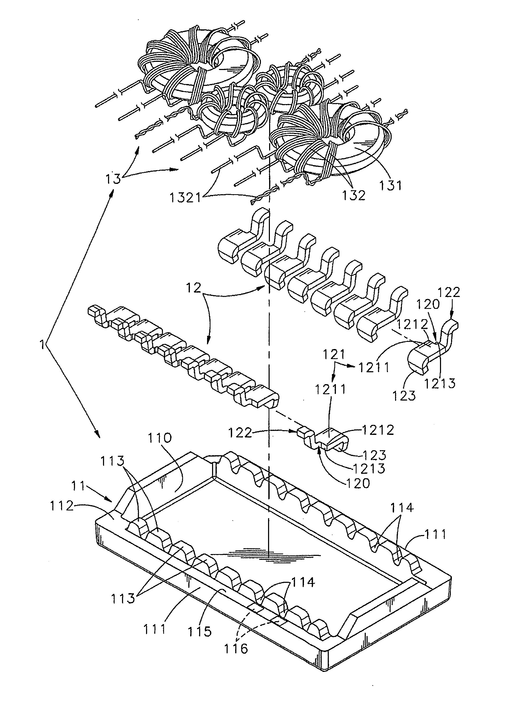
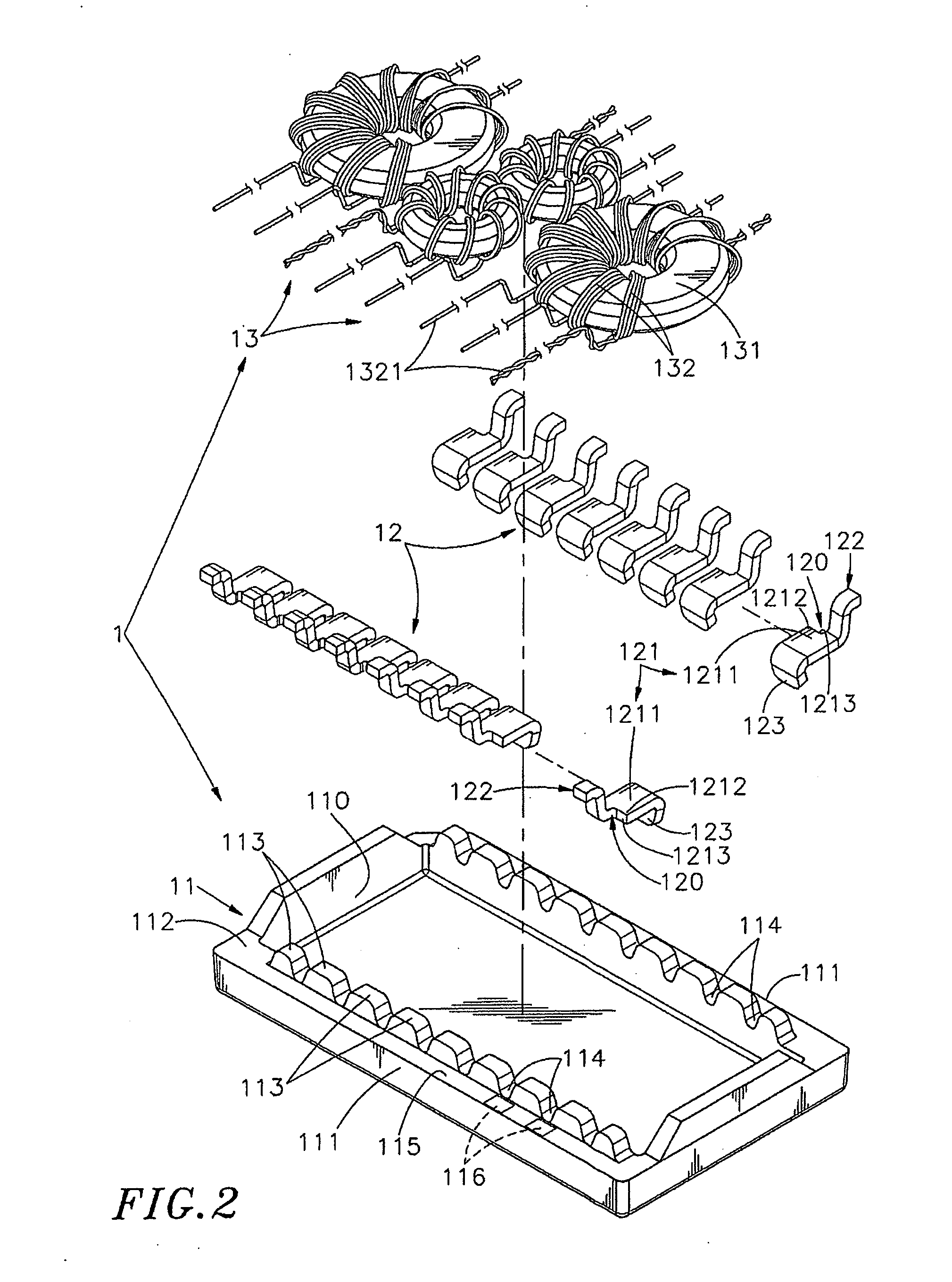
[0035]Referring to FIGS. 1˜4, a chip filter 1 in accordance with the present invention is shown comprising an insulative holder base 11, a plurality of connection terminals 12, and a plurality of filter elements 13.

[0036]The insulative holder base 11 has two opposing sidewalls 111, a recessed chamber 110 defined between the two sidewalls 111, two arrays of protruding blocks 113 respectively arranged along the sidewalls 111 adjacent to the recessed chamber 110 and protruding over the flat top edge 112 of each of the sidewalls 111, a wire groove 114 defined between each two adjacent protruding blocks 113 of each array of protruding blocks 113, a finished surface 115 formed on the flat top edge 112 of each of the sidewalls 111, and a plurality of soldering zones 116 defined in the finished surface 115 corresponding to the wire grooves 114.

[0037]The connection terminals 12 are bonded to the sidewalls 111 corresponding to the protruding blocks 113 during injection molding of the insulati...

second embodiment

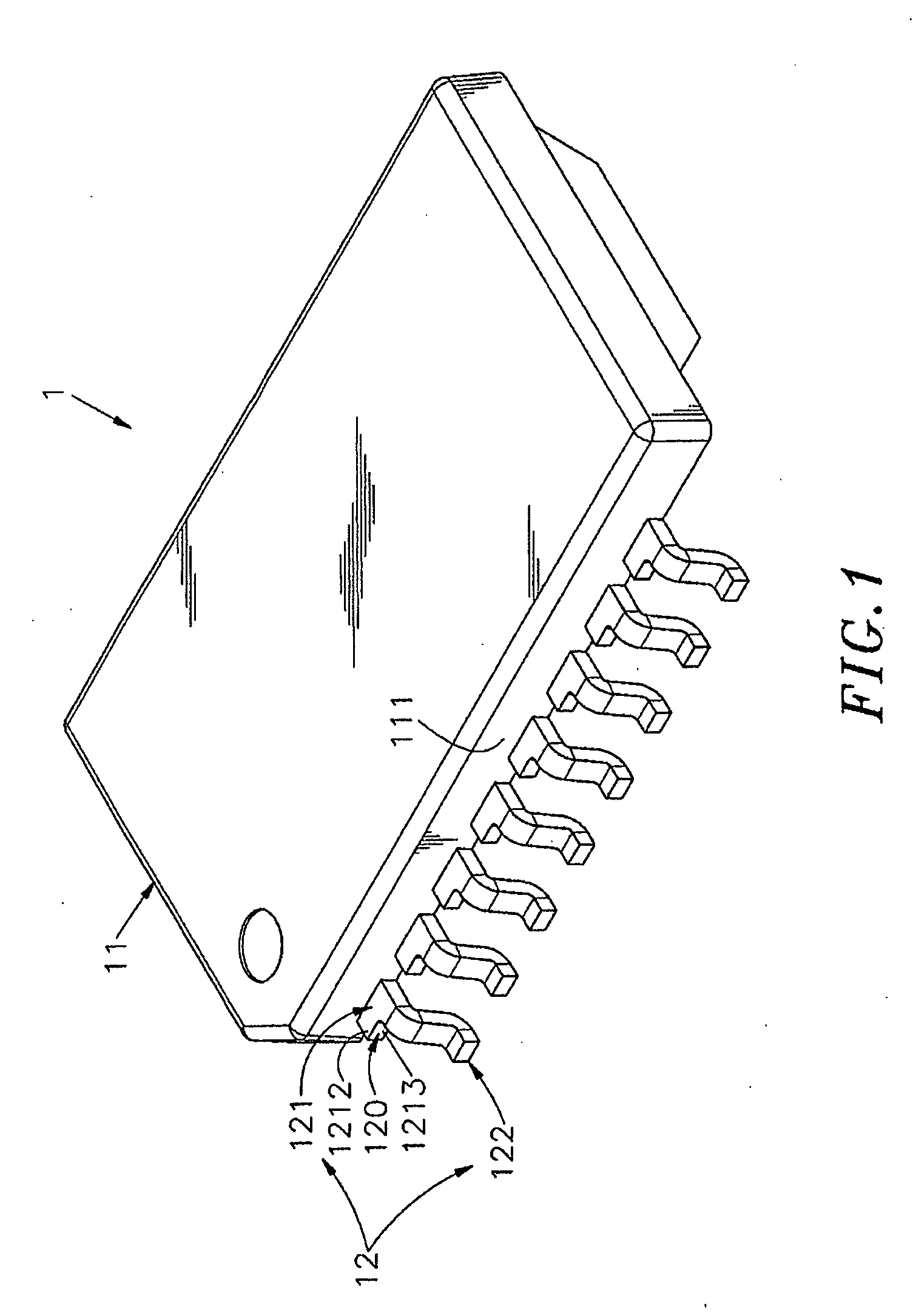
[0042]FIGS. 6 and 7 illustrate a chip filter in accordance with the present invention. According to this alternate form, each connection terminal 12 comprises a base portion 121 bonded to one sidewall 111 corresponding to the location of one soldering zone 116 in the finished surface 115 of the associating sidewall 111, a soldering surface 1211 located on the base portion 121 and kept in flush with the top edge 112 of the associating sidewall 111, a bonding tip 122 extended from the base portion 121 out of the associating sidewall 111 for bonding to one respective surface contact 21 at an external circuit board 2 (see FIG. 7). The bonding tip 122 is generally inverted U-shaped having a vertical segment 1221 connected to the base portion 121 and embedded in the associating sidewall 111, a transverse segment 1222 extended from one end of the vertical segment 1221 remote from the base portion 121 to the outside of the associating sidewall 111, a supporting segment 1223 vertically downw...


PUM


Abstract

A chip filter and supplementary tool combination is disclosed. The chip filter includes a insulative holder base having two arrays of wire grooves arranged along two opposing sidewalls thereof and soldering zones defined in a finished surface on each sidewall corresponding to the wire grooves, connection terminals each having a base portion respectively embedded in the soldering zones in the sidewalls of the insulative holder base and a soldering surface respectively kept in flush with the top edge of the associating sidewall, and filter elements having lead wires thereof respectively extending out of the insulative holder base through the wire grooves and respectively rested on the soldering surfaces of the connection terminals and held down in position by the supplementary tool for soldering by an automatic soldering machine.

Description

[0001]This application is a Continuation-In-Part of application Ser. No. 12 / 461,835, filed on Aug. 26, 2009, now pending. The patent application identified above is incorporated here by reference in its entirety to provide continuity of disclosure.BACKGROUND OF THE INVENTION[0002]1. Field of the Invention[0003]The present invention relates to chip filter fabrication technology and more particularly, to a chip filter and supplementary tool, which facilitates bonding the lead wires of filter elements of the chip filter to the respective connection terminals, saving much labor and time and improving the productivity.[0004]2. Description of the Related Art[0005]Following development of electronic information products toward fine and delicate design, SMT (Surface Mount Technology) is commonly used for the bonding of electronic components to a circuit board. Further, during signal transmission of a network interface component, for example, RJ-45 Connector, it may cause an electromagnetic ...

Claims


Application Information

Patent Timeline
Patent Type & Authority Applications(United States)
IPC IPC(8): H03H7/01
CPCH01F17/062H01F27/027H01F27/292H01F41/10H01F2005/043H05K2201/10287H01R13/719H03H2001/0092H05K3/3426H05K2201/1003H05K2201/1006H01R13/6633Y02P70/50
Inventor CHEN, PO-JUNG
Owner U D ELECTRONIC CORP
Why Eureka
Try Eureka