Miniature multi-frequency antenna

a multi-frequency antenna, miniature technology, applied in the direction of antenna details, electrically short antennas, antennas, etc., can solve the problem of resonant frequency deviation of antennas, and achieve the effect of reducing the size of the antenna and less mutual interferen

Active Publication Date: 2011-04-28
UNICTRON TECH CORP
View PDF7 Cites 33 Cited by
  • Summary
  • Abstract
  • Description
  • Claims
  • Application Information

AI Technical Summary

Benefits of technology

The objective of the present invention is to provide a miniature multi-frequency antenna that is capable of transmitting and receiving signals at more than two frequency bands. For the lower frequency band, a plurality of electrodes partially overlapped each other to form at least one particular region with specific capacitance and to adjust a reso

Problems solved by technology

However, the PIFA is susceptible to the reactance effect of nearby dielectric materials (for example, human body) and results in the resonant frequ

Method used


Image

  • Miniature multi-frequency antenna
  • Miniature multi-frequency antenna
  • Miniature multi-frequency antenna

Examples


first embodiment

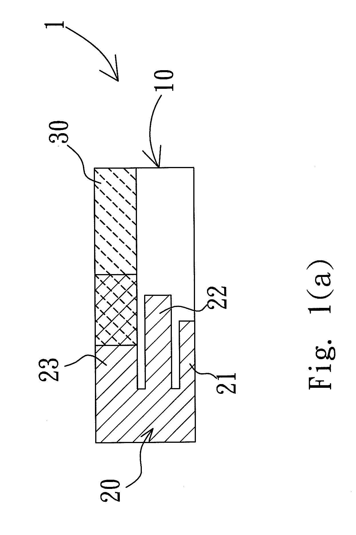
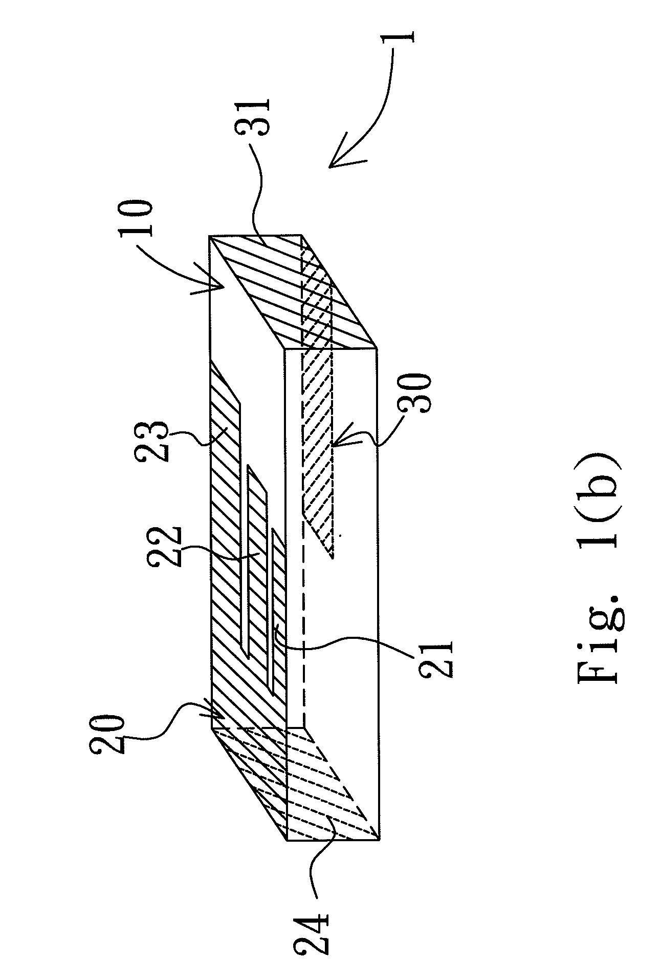
Refer to FIG. 1(a) and FIG. 1(b) for a top and a perspective view of a miniature multi-frequency antenna according to the present invention. In the following mentioned embodiments, identical number will be used for similar element. As shown in FIG. 1(a) and FIG. 1(b), a miniature multi-frequency antenna 1, comprises a substrate 10; a signal electrode 20 and a ground electrode 30. The substrate 10 has a top surface, a bottom surface and two end surfaces. The signal electrode 20 has three branches 21, 22, and 23, is disposed on the top surface of the substrate 10 and connects with a first terminal electrode 24 that is mounted on one end surface of the substrate 10. The ground electrode 30 is disposed on the bottom surface of the substrate 10, with its width roughly as same as that of branch 23 and is located below and connects with a second terminal electrode 31 that is mounted on the other end surface of substrate 10. As shown in FIG. 1(a), the ground electrode 30 is partially overla...

third embodiment

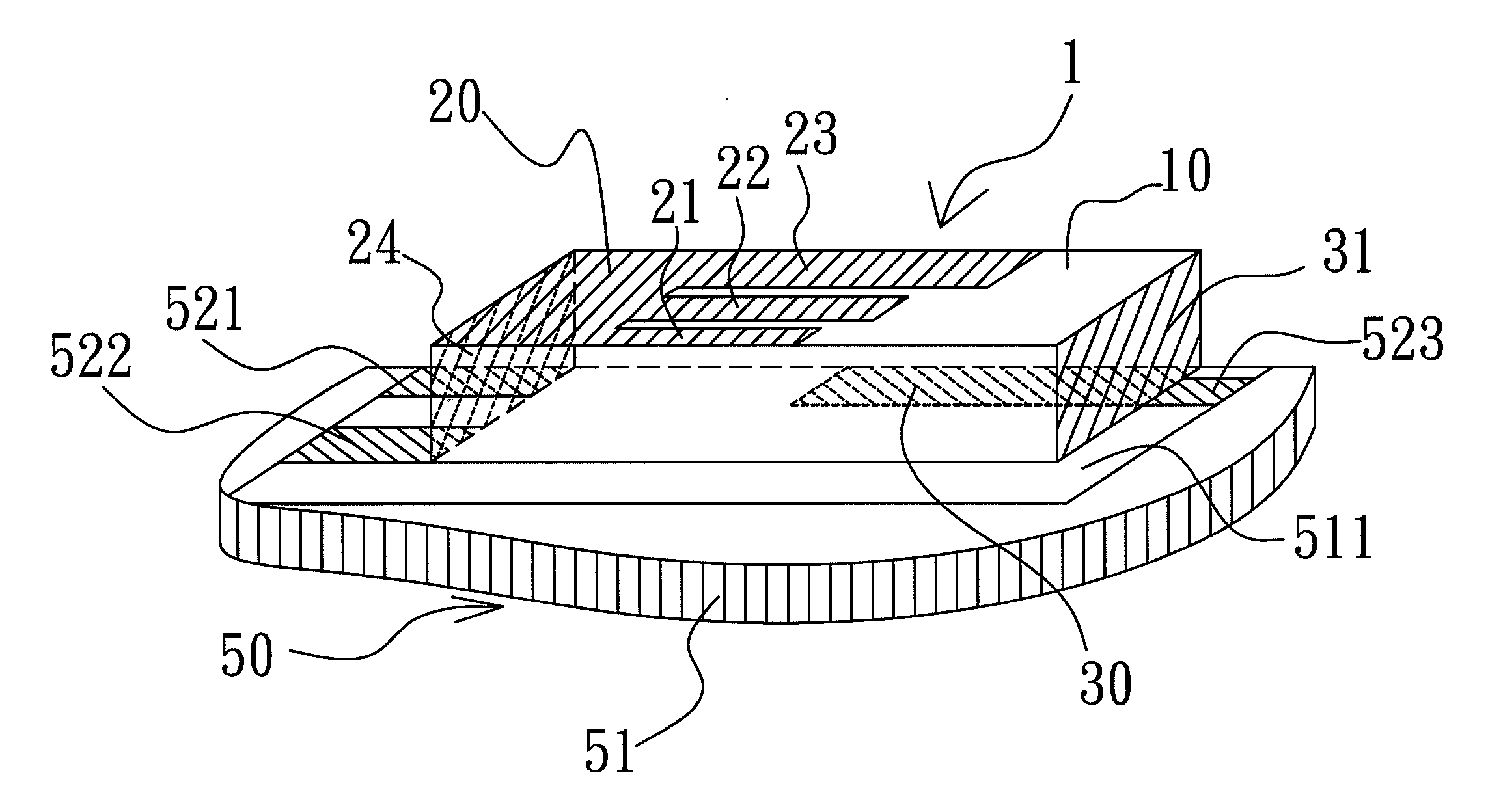
Refer to FIG. 4(a) and FIG. 4(b) for a top and a bottom view, respectively, of a miniature multi-frequency antenna according to the present invention. The circuit board 50 is formed of substrate 51 and a circuit (not shown) that is arranged on the substrate 51. The circuit board 50 comprises a clearance region 511 without deploying the circuit on substrate 51. In this embodiment, the clearance region 511 of the circuit board 50 is utilized as a substrate 10. While forming circuit on the circuit board 50, a signal electrode 20 and a ground electrode 30 are formed, respectively, on the top and bottom surface of the substrate 51 by utilizing electroplating, thick film process, thin film process, or by adhering conductive sheets. With this kind of arrangement, the volume occupied by antenna 1 becomes indiscernible, thus not only overcomes the shortcomings of the prior art but also reduces the number of manufacturing processes required in integrating the antenna 1 and the circuit board 5...

fourth embodiment

Refer further to FIGS. 5(a), 5(b) and 6 for a top, a bottom and a cross section view along A-A′ line in FIG. 5(a) and FIG. 5(b) of a miniature multi-frequency antenna according to the present invention. This embodiment is deployed by integrating antenna with a multilayer printed circuit board. As shown in FIG. 6, the substrate 51 of the circuit board 50 is a multilayered structure has multiple stacked substrate units 512 and 513. A clearance region 511 without disposing circuits, ground plane or any other electronic components, is reserved on the circuit board 50 when deploying circuits on the substrate 51. Two conductive through holes 514 and 515 are separated by a pre-determined distance and are provided in the clearance region 511 of the substrate 51 for connecting circuits on various layers. The miniature multi-frequency antenna 1 in this embodiment also utilizes the clearance region 511 of the substrate 51 as substrate 10. As such, along with the steps of manufacturing circuits...


PUM


Abstract

A miniature multi-frequency antenna, comprising at least one dielectric substrate, at least one signal electrode and at least one ground electrode. The signal electrode and the ground electrode are disposed on a substrate. The signal electrode contains at least two branches and at least one branch is partially overlapped with the ground electrode. Each interlayer region between the partially overlapped electrodes forms a specific capacitance. By utilizing this interlayer capacitive effect, the resonant frequency of lower frequency band is achieved while the size of the antenna is effectively reduced. For obtaining the resonant frequency of the high frequency bands, the design concept of PIFA is applied on other branches of the signal electrode. A miniature antenna thus obtained is capable of transmitting/receiving multi-frequency signals having the benefits of easily adjusting impedance and resonant frequency.

Description

BACKGROUND OF THE INVENTION1. Field of the InventionThe present invention relates to an antenna, particularly to a miniature multi-frequency antenna, that is suitable for being utilized in small-sized communication devices and is capable of receiving and transmitting multi-frequency signals.2. The Prior ArtsNowadays, an antenna plays an important role in various wireless communication electronic devices. With the progress and development of Integrated Circuit (IC) technology, various electronic elements have been miniaturized. Thus, the trend for the development of wireless communication devices is toward light weight, thin profile and compact size while still providing various functions such as data processing, network connection, voice signals transmitting / receiving, audio / video signals broadcasting, etc. Therefore, it is preferred to have a small-sized antenna with the capability of transmitting and receiving multi-frequency signals.In general, a Planar Inverted F Antenna (PIFA) ...

Claims


Application Information

Patent Timeline
IPC IPC(8): H01Q1/38H01Q5/00H01Q5/371
CPCH01Q5/371H01Q9/0421
Inventor CHOU, CHIH-SHEN
Owner UNICTRON TECH CORP
Why Eureka
Try Eureka