
Temporary Memory Circuits for Matrix Display Device

Inactive Publication Date: 2011-04-28
MICROEMISSIVE DISPLAY
View PDF12 Cites 1 Cited by
  • Summary
  • Abstract
  • Description
  • Claims
  • Application Information

AI Technical Summary

Benefits of technology

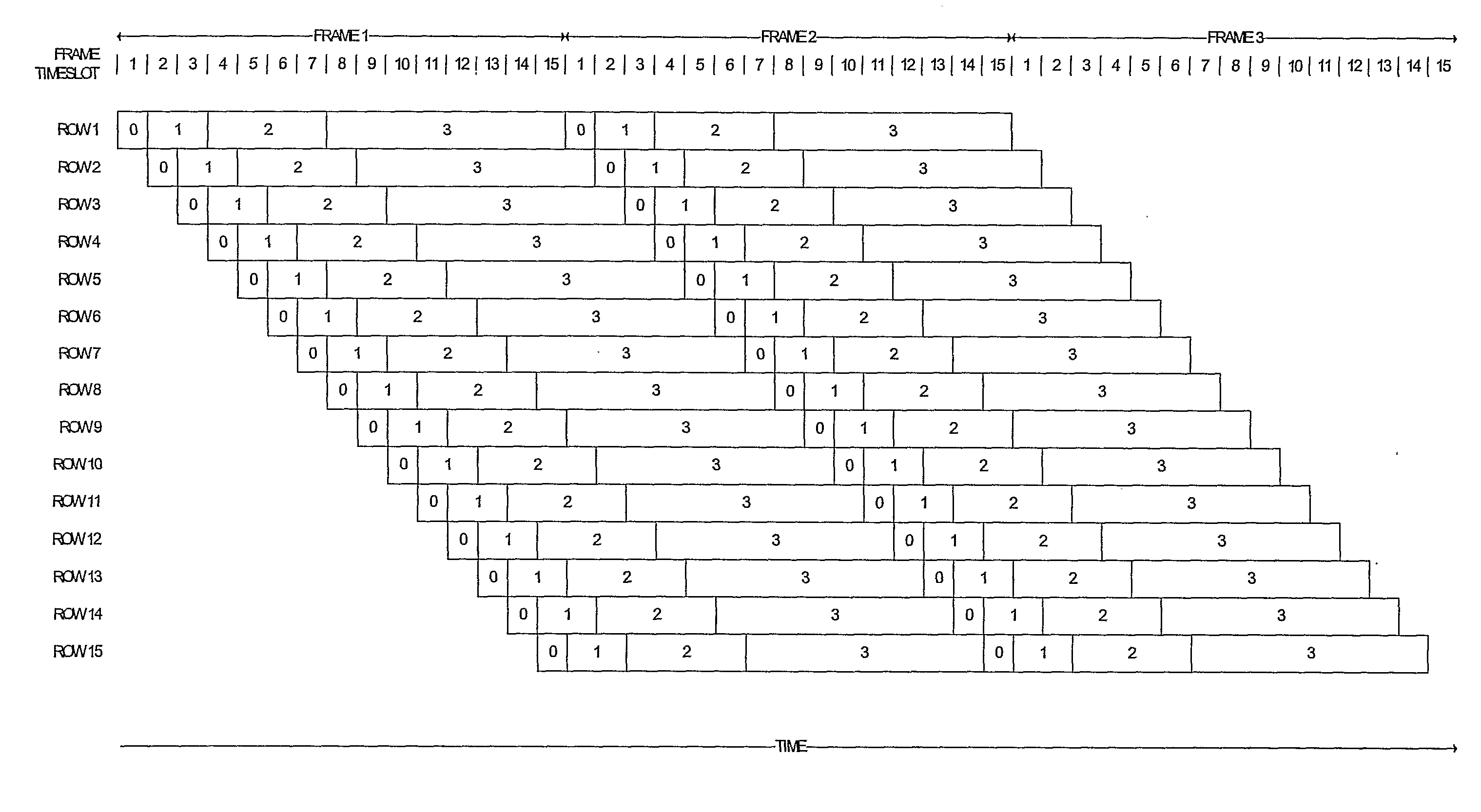
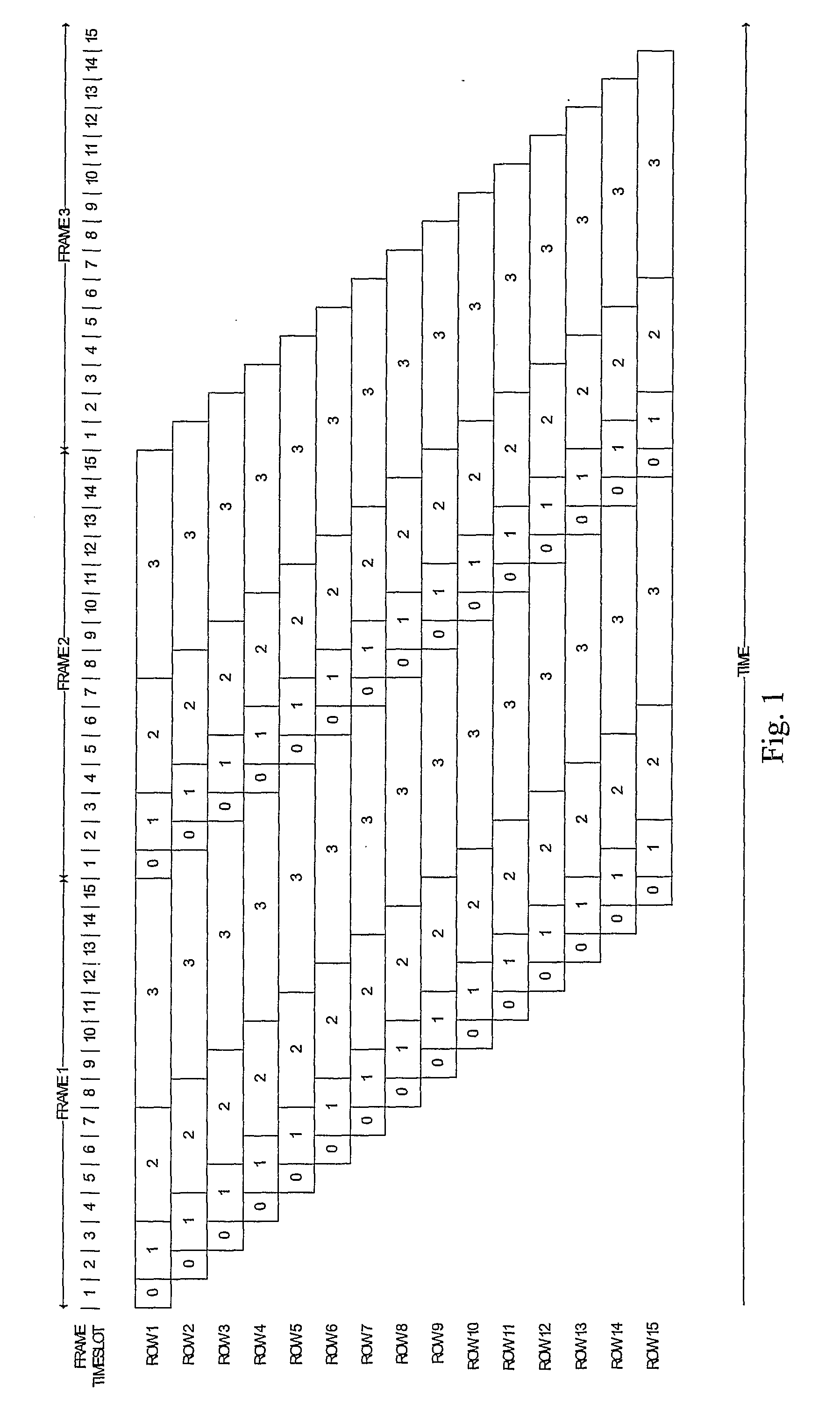
[0014]It is an aim of the present invention to provide a circuit and method for driving electronic display pixels with a temporary memory store with much reduced memory requirements, while still maintaining high apparent bit depth greyscale.

Problems solved by technology

In the context of organic light emitting device (OLED) microdisplays, a digital approach to controlling the small currents required is favored as it is extremely difficult to successfully control greyscale in microdisplay pixels by varying the current magnitude.
A complication is that bitplane data must be read out of the temporary memory store in a bursty manner, in order to use up as small a proportion of the frame time as possible.
This typically results in increased operating frequency and power dissipation for the electronic display system.
A further complication is that the temporary memory store typically holds data for two complete frames.
If implemented on-chip, it can occupy quite a significant proportion of the overall chip size.
However, this increases the area requirements of the pixel, and thus the cost of the display component.
However, the main disadvantage of this approach is that storing the bits in the pixel increases the area requirements of the pixel, and thus the cost of the display component.

Method used


Image

  • Temporary Memory Circuits for Matrix Display Device
  • Temporary Memory Circuits for Matrix Display Device
  • Temporary Memory Circuits for Matrix Display Device

Examples


Embodiment Construction

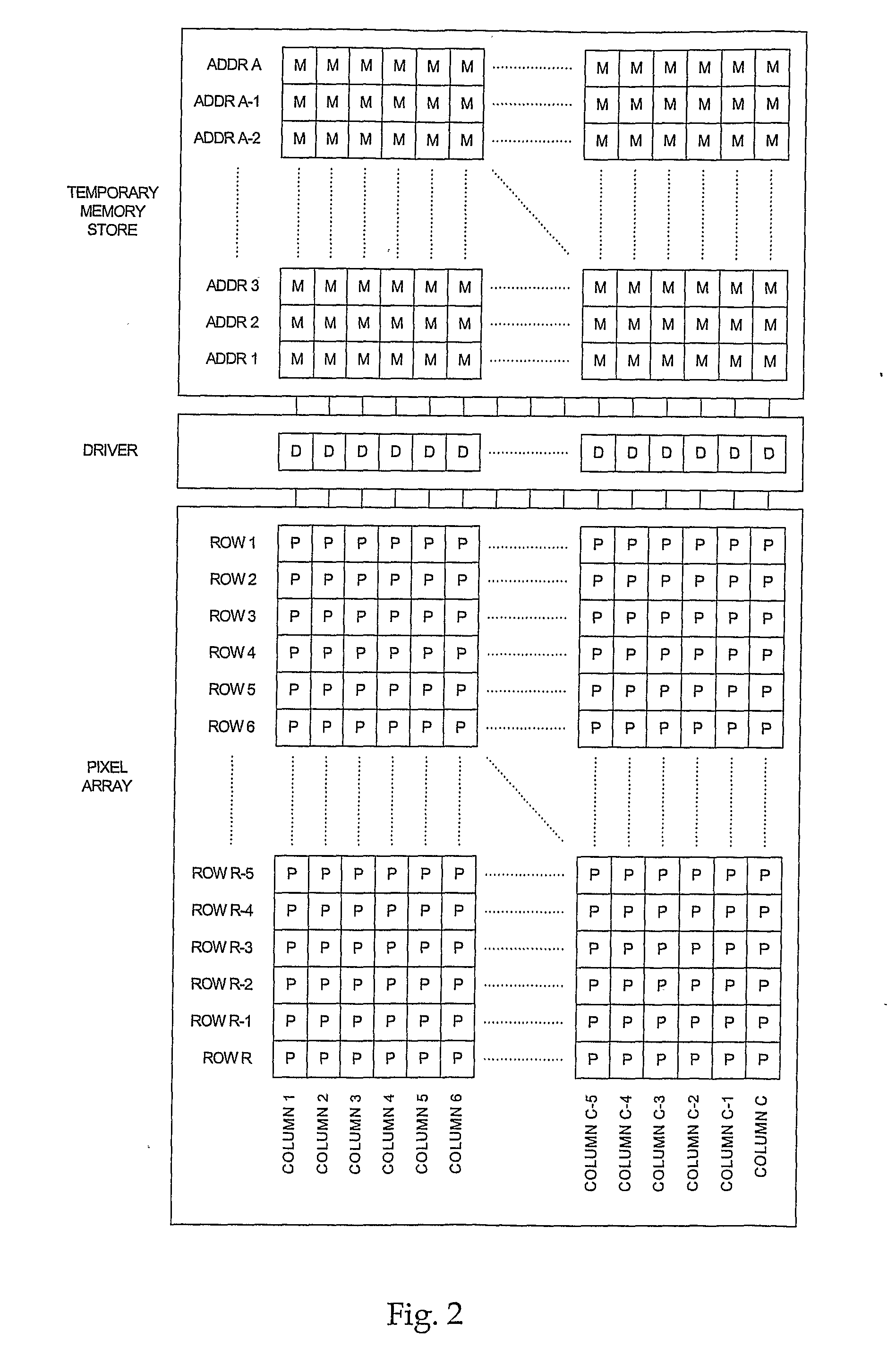
[0020]FIG. 2 shows an electronic display which comprises a pixel array 1, a temporary memory store 2, and a driver block 3. The pixel array consists of an array of pixels P with R rows and C columns. Each pixel P consists of one or more memory storage elements and an electrode driver. The pixel requires a multiplexer if the pixel has more than one memory element so that the appropriate memory element can be selected and passed as a control signal to the pixel electrode driver. The pixel electrode driver, in turn, provides a signal to control the pixel's electrode to emit or modulate light.

[0021]The temporary memory store 2 consists of a plurality of memory elements. These memory elements may be arranged in rows, designated ADDR1 to ADDR A, each with C memory elements. The number of rows A in the temporary memory store depends on the required PWM grey level bit depth, and the number of rows in the pixel array. If the required bit depth is N, then it is convenient to partition the tem...


PUM


Abstract

A circuit for supplying video data supplied in frames divided into timeslots to an array of pixels comprises a plurality of one-bit temporary storage elements (M), at least some of which are arranged to store data for different pixels of the array during different timeslots within a frame. The circuit can be used in an electroluminescent display in which each pixel (P) comprises an organic light-emitting diode.

Description

BACKGROUND TO THE INVENTION[0001]This invention relates to optoelectronic display apparatus. The invention provides circuits for temporary storage of frames of data prior to display thereof.[0002]A known electronic display, and in particular a microdisplay, consists of an array of individually addressable picture elements (pixels). In some applications, these arrays function in binary mode, where each individual pixel receives either an ON or OFF signal. The signal at the pixel is used to modulate or emit light via an overlying electro-optic material. Typically, the pixels of the array that receive the ON signal form the image the viewer receives, either directly, or magnified via some optics.[0003]In the context of organic light emitting device (OLED) microdisplays, a digital approach to controlling the small currents required is favored as it is extremely difficult to successfully control greyscale in microdisplay pixels by varying the current magnitude. By using a digital approac...

Claims


Application Information

Patent Timeline
IPC IPC(8): H04N9/64H05B44/00
CPCG09G3/2022G09G3/2092G09G2360/18G09G5/42G09G3/3208G09G3/20
Inventor BURNS, DWAYNE CHARLESWOODBURN, ROBERT JOHNSTONENEWSAM, MARK IANHURWITZ, JONATHAN EPHRAIM DAVID
Owner MICROEMISSIVE DISPLAY
Learn More