
Light-emitting device and fabricating method thereof

Active Publication Date: 2011-05-05
SUZHOU LEKIN SEMICON CO LTD
View PDF9 Cites 28 Cited by
  • Summary
  • Abstract
  • Description
  • Claims
  • Application Information

AI Technical Summary

Benefits of technology

[0018]The embodiment can provide a light emitting device having a novel structure and a method of manufacturing the same.
[0019]The embodiment can provide a light emitting device capable of improving electrical characteristics and a method of manufacturing the same.
[0020]The embodiment can provide a light emitting device capable of improving light efficiency and a method of manufacturing the same.

Problems solved by technology

In addition, according to the lateral type LED, since the first conductive semiconductor layer, the active layer and the second conductive semiconductor layer are formed over the growth substrate having low thermal conductivity, the heat dissipation is not easy.
Third, in the vertical type LED, when the light emitting semiconductor layer is bonded to the conductive support substrate through a wafer bonding process, cracks or breakages may be caused in the light emitting semiconductor layer due to the difference in a thermal expansion coefficient between the light emitting semiconductor layer and the conductive support substrate.
Accordingly, the wafer bonding process has to be performed at a temperature of less than 300° C. to minimize the thermal stress, so that it is difficult to perform the subsequent processes.

Method used


Image

  • Light-emitting device and fabricating method thereof
  • Light-emitting device and fabricating method thereof
  • Light-emitting device and fabricating method thereof

Examples


first embodiment

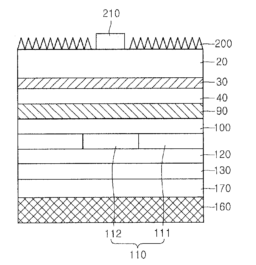
[0035]FIG. 1 is a sectional view showing a light emitting device according to a

[0036]Referring to FIG. 1, first and second wafer bonding layers 130 and 170 are formed over a support substrate 160, and a diffusion barrier layer 120 is formed over the first wafer bonding layer 130.

[0037]A second electrode layer 110 including a reflective current spreading layer 111 and a current blocking layer 112 is formed over the diffusion barrier layer 120, and a current injection layer 100 is formed over the second electrode layer 110.

[0038]In addition, a superlattice structure layer 90 is formed over the current injection layer 100, and a light emitting semiconductor layer including a second conductive semiconductor layer 40, an active layer 30, and a first conductive semiconductor layer 20 is formed over the superlattice structure layer 90.

[0039]In addition, a light extracting structure layer 200 and a first electrode layer 210 are formed over the first conductive semiconductor layer 20

[0040]In...

second embodiment

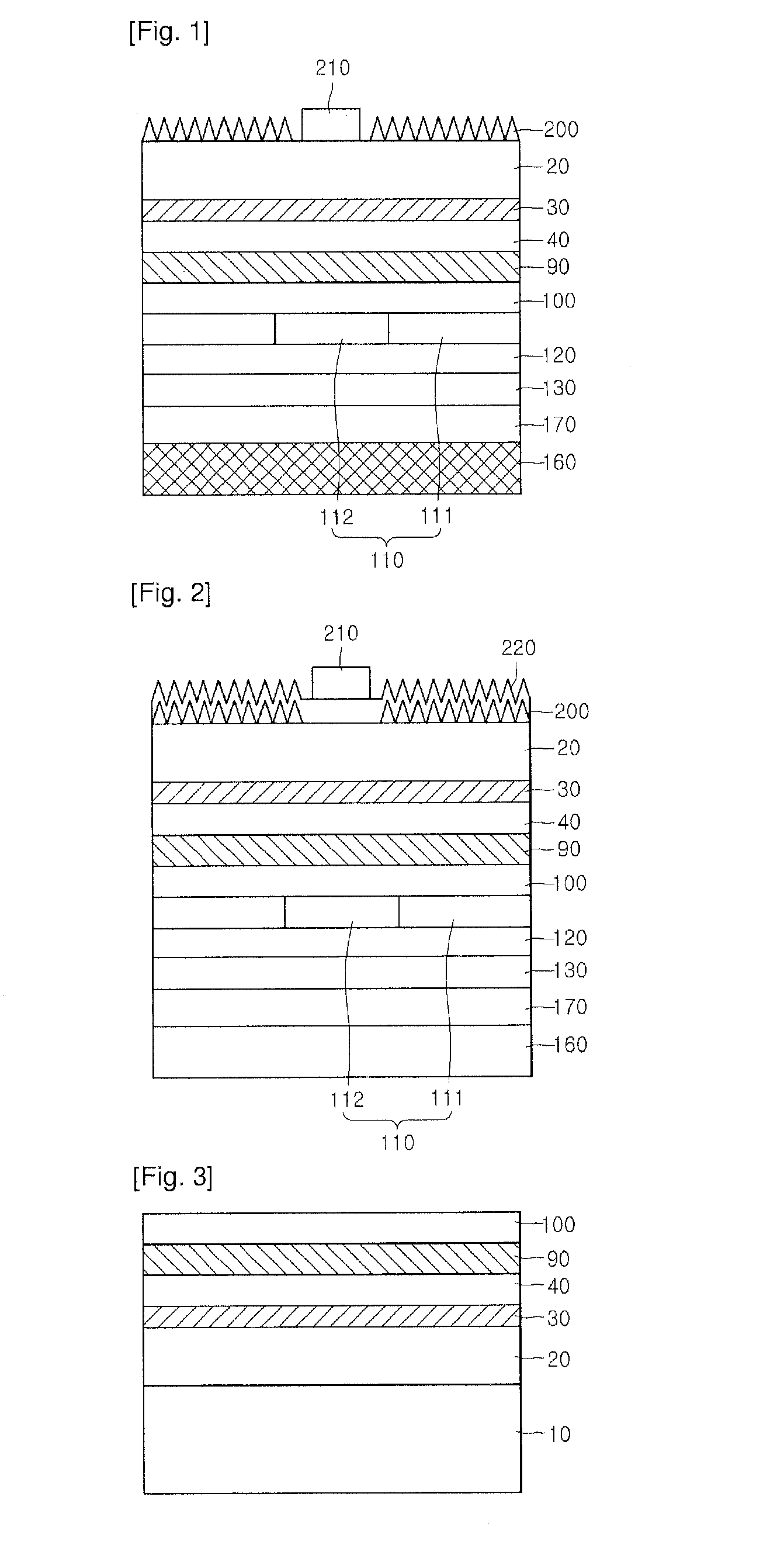
[0059]FIG. 2 is a sectional view showing a light emitting device according to a

[0060]The light emitting device according to the second embodiment shown in FIG. 2 has a structure similar to that of the light emitting device according to the first embodiment. Accordingly, the light emitting device according to the second embodiment will be described while focusing over the difference from the first embodiment in order to avoid redundancy.

[0061]In the light emitting device according to the second embodiment, after forming a first ohmic contact electrode layer 220 over the first conductive semiconductor layer 20 and the light extracting structure layer 200, the first electrode layer 210 is formed over the first ohmic contact electrode layer 220.

[0062]The first ohmic contact electrode layer 220 is provided over a top surface thereof with a concavo-convex structure so that the light emitted from the active layer 30 can be effectively extracted to the outside.

[0063]The first ohmic contact ...

third embodiment

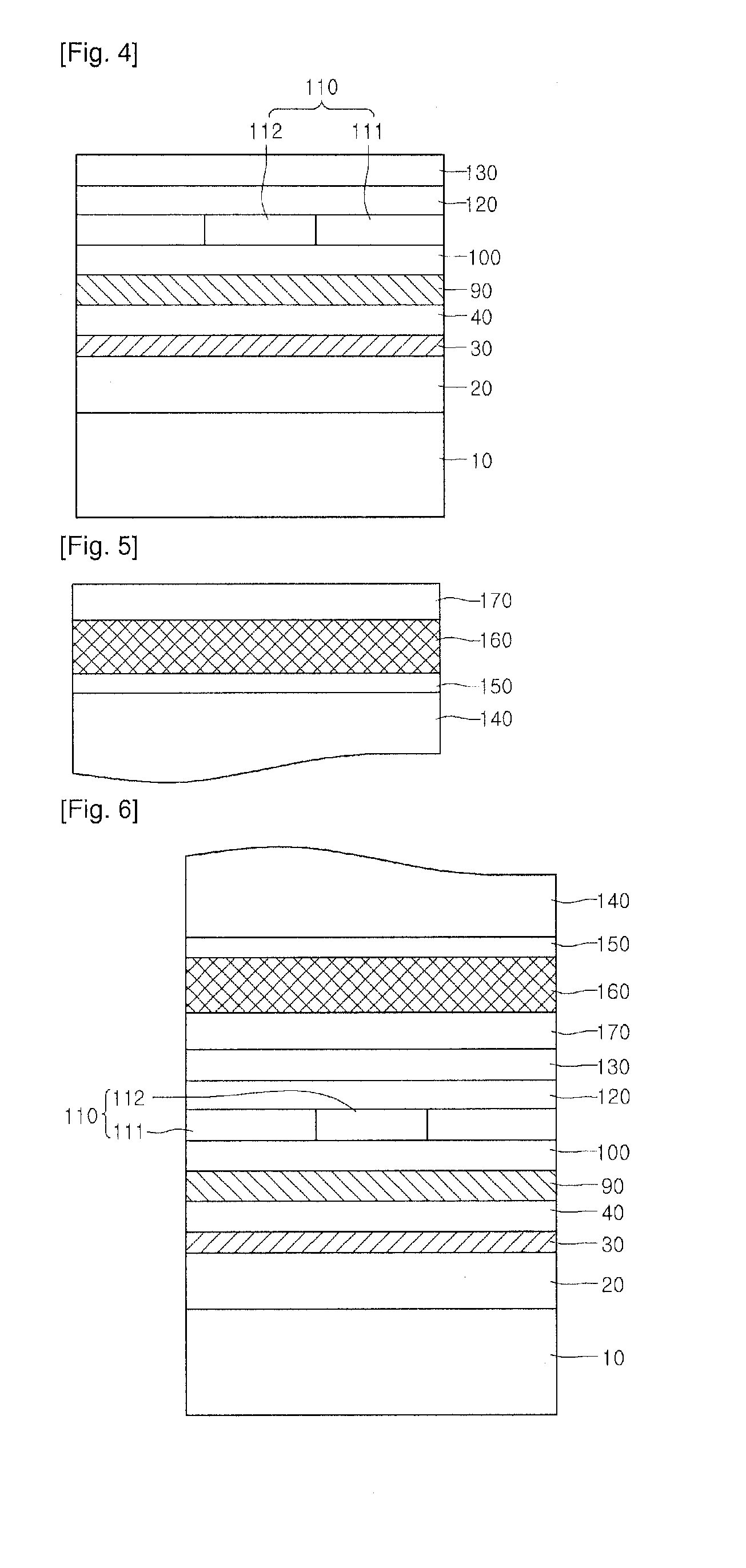
[0096]FIG. 12 is a sectional view showing a light emitting device according to a

[0097]The light emitting device according to the third embodiment will be described while focusing over the difference from the first embodiment in order to avoid redundancy.

[0098]Referring to FIG. 12, the second wafer bonding layer 170 is formed over the support substrate 160, and a current blocking layer 250 and the first wafer bonding layer 130 are formed over the second wafer bonding layer 170. In addition, the diffusion barrier layer 120 is formed over the first wafer bonding layer 130.

[0099]The first wafer bonding layer 130 and the diffusion barrier layer 120 are arranged at a lateral surface of the current blocking layer 250.

[0100]The reflective current spreading layer 111 is formed over the diffusion barrier layer 120 and the current blocking layer 250, and the current injection layer 100 is partially formed over the reflective current spreading layer 111. The current injection layer 100 is forme...


PUM


Abstract

Disclosed are a light emitting device and a method of manufacturing the same. The light emitting device includes a support substrate, a wafer bonding layer over the support substrate, a second electrode layer, which includes a current blocking layer and a reflective current spreading layer, over the wafer bonding layer, a current injection layer over the second electrode layer, a superlattice structure layer over the current injection layer, a second conductive semiconductor layer over the superlattice structure layer, an active layer over the second conductive semiconductor layer, a first conductive semiconductor layer over the active layer, and a first electrode layer over the first conductive semiconductor layer.

Description

TECHNICAL FIELD[0001]The embodiment relates to a light emitting device and a method of manufacturing the same.BACKGROUND ART[0002]Recently, a light emitting diode (LED) is spotlighted as a light emitting device. Since the LED can convert electric energy into light energy with high efficiency and long life span of about 5 years or more, the LED can remarkably reduce the energy consumption and repair and maintenance cost. In this regard, the LED is spotlighted in the next-generation lighting field.[0003]Such an LED includes a light emitting semiconductor layer including a first conductive semiconductor layer, an active layer and a second conductive semiconductor layer, in which the active layer generates light according to current applied to the first and second conductive semiconductor layers.[0004]The LED may be classified into a lateral type LED and a vertical type LED.[0005]According to the lateral type LED, the first conductive semiconductor layer, the active layer and the second...

Claims


Application Information

Patent Timeline
IPC IPC(8): H01L33/04H01L33/00H01L33/14H01L33/40
CPCH01L33/0079H01L33/145H01L33/42H01L33/04H01L33/405H01L33/0093
Inventor SONG, JUNE O
Owner SUZHOU LEKIN SEMICON CO LTD
Features
  • Generate Ideas
  • Intellectual Property
  • Life Sciences
  • Materials
  • Tech Scout
  • Unparalleled Data Quality
  • Higher Quality Content
  • 60% Fewer Hallucinations
Learn More