Non-linear element, display device, and electronic device

a display device and non-linear technology, applied in the direction of basic electric elements, semiconductor devices, electrical equipment, etc., to achieve the effect of large on-state current, small off-state current, and large on-state curren

Inactive Publication Date: 2011-05-05
SEMICON ENERGY LAB CO LTD
View PDF34 Cites 25 Cited by
  • Summary
  • Abstract
  • Description
  • Claims
  • Application Information

AI Technical Summary

Benefits of technology

[0008]An embodiment of the present invention provides a non-linear element (e.g., a diode) which can be miniaturized and includes a field effect transistor (for example, a thin film transistor) that can be manufactured at low process temperature and has large on-state current and small off-state current. A non-linear element includes a first electrode provided over a substrate, an oxide semiconductor film provided on and in contact with the first electrode and purified, a second electrode provided on and in contact with the oxide semiconductor film, a gate insulating film covering the first electrode, the oxide semiconductor film, and the second electrode, and third electrodes provided in contact with the gate insulating film and facing each other with the first electrode, the oxide semiconductor film, and the second electrode interposed therebetween or a third electrode provided in contact with the gate insulating film and surrounding the second electrode. In the non-linear element, the third electrodes or the third electrode are / is connected to the first electrode or the second electrode, and a current flows between the first electrode and the second electrode.
[0009]With a field effect transistor (for example, a thin film transistor) which can be miniaturized and has large on-state current and small off-state current, it is possible to obtain a diode which has very small reverse current. Accordingly, a diode which is resistant to a breakdown (i.e., has high withstand voltage) can be manufactured.

Problems solved by technology

As described above, although a non-linear element (e.g., a diode) in which silicon carbide is used is expected to have high withstand voltage and small reverse saturation current, there are many problems in manufacturing and achieving such an element.

Method used


Image

  • Non-linear element, display device, and electronic device
  • Non-linear element, display device, and electronic device
  • Non-linear element, display device, and electronic device

Examples


embodiment 1

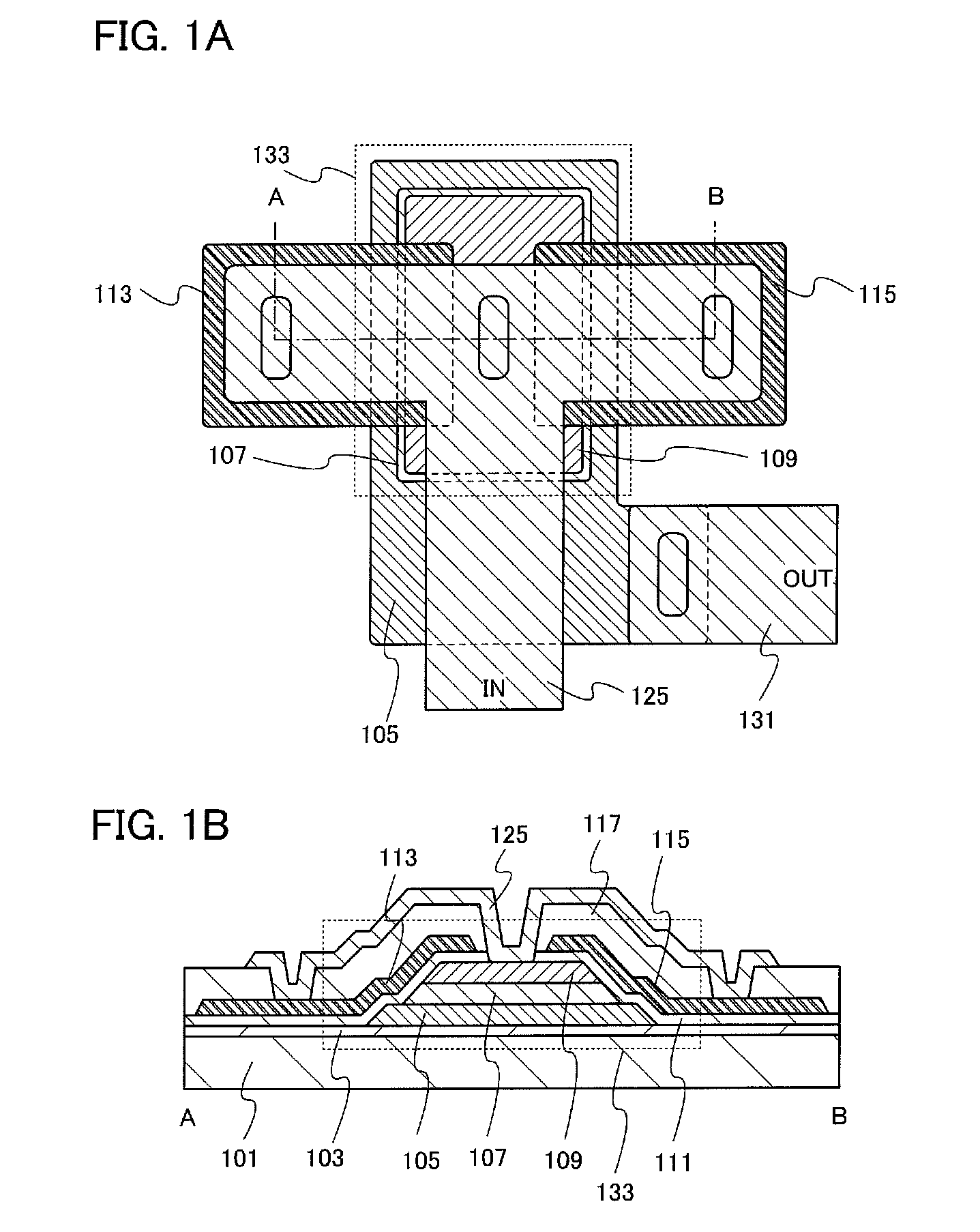
[0025]In this embodiment, an example of a structure of a diode which is one embodiment of the present invention will be described with reference to FIGS. 1A and 1B. The diode which is described in this embodiment can be obtained by connecting a source or a drain of a field effect transistor, for example, a thin film transistor to a gate thereof.

[0026]In the diode illustrated in FIGS. 1A and 1B, a wiring 125 is connected to a third electrode 113, a third electrode 115, and a second electrode 109, and the second electrode 109 is connected to a first electrode 105 through an oxide semiconductor film 107. The first electrode 105 is connected to a wiring 131.

[0027]FIG. 1A is a top view of a diode-connected thin film transistor 133. FIG. 1B is a cross-sectional view along dashed-and-dotted line A-B in FIG. 1A.

[0028]As illustrated in FIG. 1B, the first electrode 105, the oxide semiconductor film 107, and the second electrode 109 are stacked over an insulating film 103 which is formed over ...

embodiment 2

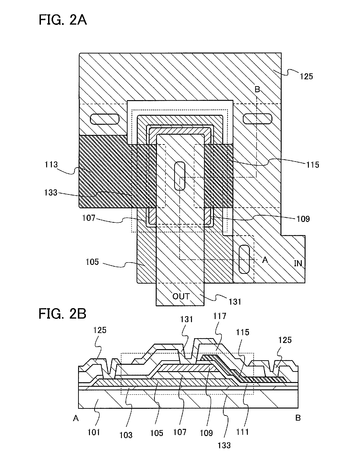
[0053]In this embodiment, an example of a diode having a structure different from that in Embodiment 1 will be described with reference to FIGS. 3A and 3B. The diode which is described in this embodiment can be obtained by connecting a source or a drain of a field effect transistor, for example, a thin film transistor to a gate thereof.

[0054]In the diode illustrated in FIGS. 3A and 3B, a wiring 131 is connected to a first electrode 105 and a third electrode 113, and a wiring 132 is connected to a first electrode 106 and a third electrode 115. The first electrode 105 and the first electrode 106 are connected to a second electrode 109 through an oxide semiconductor film 107. The second electrode 109 is connected to a wiring 129.

[0055]FIG. 3A is a top view of diode-connected thin film transistors 141 and 143. FIG. 3B is a cross-sectional view along dashed-and-dotted line A-B in FIG. 3A.

[0056]As illustrated in FIG. 3B, the first electrode 105 and the first electrode 106, the oxide semic...

embodiment 3

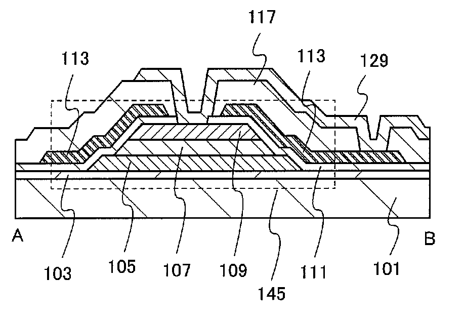
[0067]In this embodiment, an example of a diode, which is an embodiment of the present invention and has a structure different from those in Embodiments 1 and 2, will be described with reference to FIGS. 5A and 5B. The diode which is described in this embodiment can be obtained by connecting a source or a drain of a field effect transistor, for example, a thin film transistor to a gate thereof.

[0068]In the diode illustrated in FIGS. 5A and 5B, a wiring 131 is connected to a first electrode 105 and a third electrode 113. The first electrode 105 is connected to a second electrode 109 through an oxide semiconductor film 107. The second electrode 109 is connected to a wiring 129.

[0069]FIG. 5A is a top view of a diode-connected thin film transistor 145. FIG. 5B is a cross-sectional view along dashed-and-dotted line A-B in FIG. 5A.

[0070]As illustrated in FIG. 5B, the first electrode 105, the oxide semiconductor film 107, and the second electrode 109 are stacked over an insulating film 103...


PUM


Abstract

A non-linear element (e.g., a diode) with small reverse saturation current is provided. A non-linear element includes a first electrode provided over a substrate, an oxide semiconductor film provided on and in contact with the first electrode, a second electrode provided on and in contact with the oxide semiconductor film, a gate insulating film covering the first electrode, the oxide semiconductor film, and the second electrode, and a third electrode provided in contact with the gate insulating film and adjacent to a side surface of the oxide semiconductor film with the gate insulating film interposed therebetween or a third electrode provided in contact with the gate insulating film and surrounding the second electrode. The third electrode is connected to the first electrode or the second electrode.

Description

TECHNICAL FIELD[0001]The present invention relates to a non-linear element including an oxide semiconductor and a semiconductor device including the non-linear element, such as a display device. Furthermore, the present invention relates to an electronic device including the semiconductor device.BACKGROUND ART[0002]Among semiconductor devices, diodes are required to have high withstand voltage, small reverse saturation current, and the like. In order to meet such a requirement, a diode in which silicon carbide (SiC) is used has been researched. Silicon carbide used as a semiconductor material has a width of a forbidden band of 3 eV or more, excellent controllability of electric conductivity at high temperature, and is more resistant to dielectric breakdown than silicon. Therefore, silicon carbide is expected to be applied to a diode in which reverse saturation current is small and withstand voltage is high. For example, a Schottky barrier diode in which silicon carbide is used and r...

Claims


Application Information

Patent Timeline
Patent Type & Authority Applications(United States)
IPC IPC(8): H01L29/78H01L27/105
CPCH01L27/1225H01L29/22H01L29/42392H01L29/7869H01L29/78642H01L29/78648H01L29/7391
Inventor YAMAZAKI, SHUNPEI
Owner SEMICON ENERGY LAB CO LTD
Why Eureka
Try Eureka