Test device for liquid crystal display device and test method thereof

a liquid crystal display and test device technology, applied in the field of semiconductor integrated circuit technology, can solve problems affecting the final test, and achieve the effects of eliminating the effect of the via hole, and reducing the number of test steps

Active Publication Date: 2014-12-16
BEIHAI HKC OPTOELECTRONICS TECH CO LTD
View PDF13 Cites 2 Cited by
  • Summary
  • Abstract
  • Description
  • Claims
  • Application Information

AI Technical Summary

Benefits of technology

[0039]It can be seen from the above technical solution that, in the detection device of a liquid crystal display device provided by the present invention, the via hole between the transmission line and the shorting bar is eliminated according to the design, which eliminates line defects of the data lines or the scanning lines caused by via holes during the testing process, and thus eliminates the effect of the via holes on the test results.
[0040]In addition, the detection device of a liquid crystal display device provided by the present invention saves space for the test portion, which facilitates the production of a small size liquid crystal display device. Also, the saved space can be used for the increase of size of a thin film transistor switch, such that the thin film transistor switch has a larger ON state current thus improving display characteristics.

Problems solved by technology

Therefore, there is line defect in the data line direction or in the scanning line direction when the liquid crystal display device is tested, which will affect the final test results.

Method used


Image

  • Test device for liquid crystal display device and test method thereof
  • Test device for liquid crystal display device and test method thereof
  • Test device for liquid crystal display device and test method thereof

Examples


first embodiment

A First Embodiment

[0051]As stated in the background of the present invention, in the manufacturing process of a liquid crystal display device, larger static electricity will usually cause the conductive film at the via hole connecting the transmission line and the shorting bar to be burned, so as to produce the line defect of the data lines or scanning lines, thus affecting the final test result. The applicant has found according to the research that the essence reason causing the above phenomenon is that, shorting bars and transmission lines are formed in different steps in the prior art, therefore via holes are required to connect the shorting bars and the transmission lines, and thus the test results are affected in the testing process due to defects of via holes.

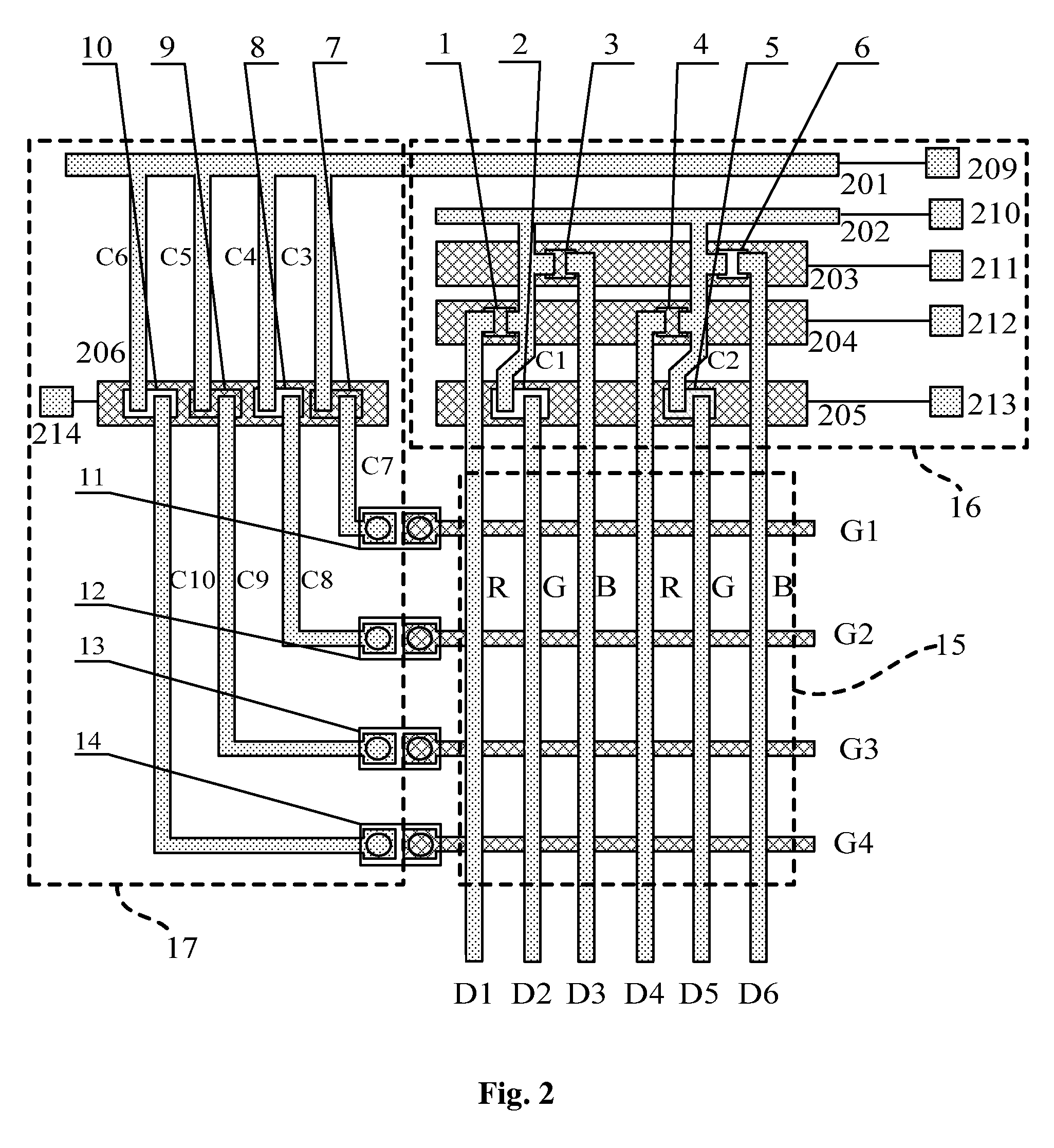
[0052]Referring to FIG. 2, FIG. 2 is a structural schematic diagram of a test device for a liquid crystal display device provided by an embodiment of the present invention. In FIG. 2, a display region 15 is shown, the ot...

second embodiment

A Second Embodiment

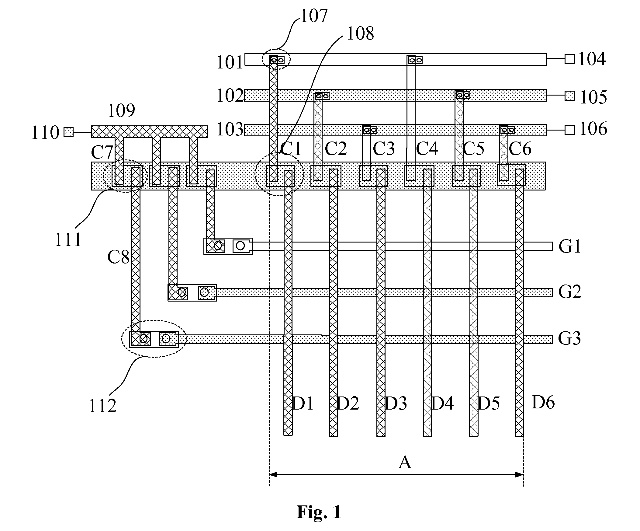
[0064]In the first embodiment, the six data lines and the three control lines have intersecting portions with larger areas, which will lead to a signal transmission delay during the transmission of a test signal or a control signal, and will slower the response speed of the testing results. In view of this, a new design is provided in the embodiment to decrease the area of the intersecting portion of the data line and the control line, so as to facilitate the transmission of signals and improve response speed.

[0065]Referring to FIG. 5, FIG. 5 is a partial structural schematic diagram of another test device for a liquid crystal display device provided by the embodiment of the present invention. On the basis of FIG. 2, in the embodiment, the width of the second control line 207 at the intersecting portions 301 of the second control line 207 and the data lines D3, D6 is designed to be smaller than the width of the second control line 207 at non-intersecting portions,...

third embodiment

A Third Embodiment

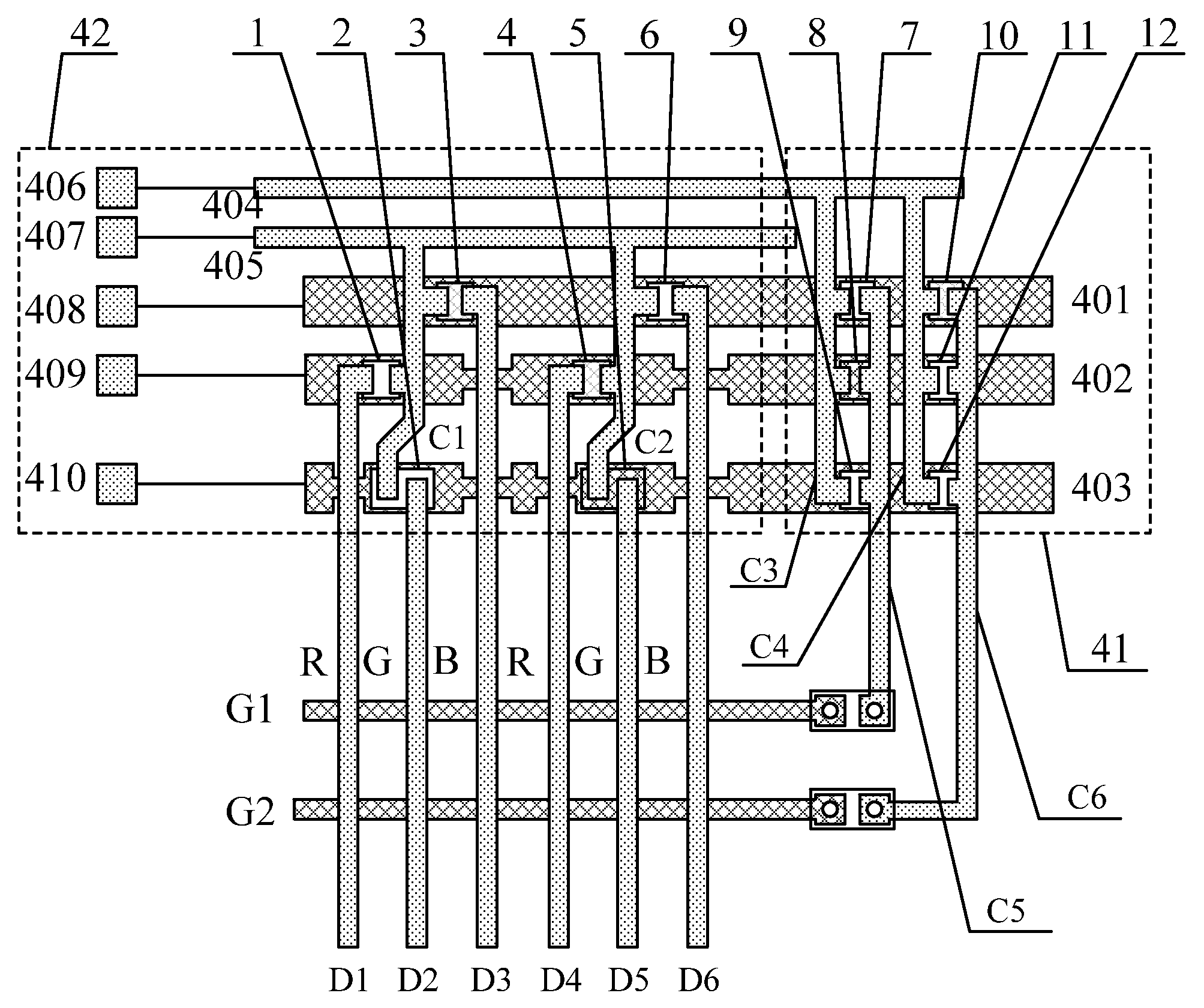
[0068]Referring to FIG. 2, in the testing process for a liquid crystal display device in the first embodiment, it is required to input corresponding testing signals or control signals to the test terminals 209, 210, 211, 212, 214 (referring to FIG. 2). It can be seen from FIG. 2 that, the test terminal 214 of the control line 206 in the scanning line test region 17 is located at a different side from the five test terminals 209, 210, 211, 212, 213 in the data line test region 16, this structure leads to a larger occupied space of the non-display region (including the data line test region 16 and the scanning line test region 17).

[0069]Based on those, the embodiment provides a new design, so as to decrease the number of test terminals, and locate all the test terminals at the same side so that the occupied space of the non-display region is decreased.

[0070]Referring to FIG. 6, FIG. 6 is a structural schematic diagram of another test device for a liquid crystal displ...


PUM

PropertyMeasurementUnit
voltageaaaaaaaaaa
voltageaaaaaaaaaa
voltageaaaaaaaaaa

Abstract

A test device for a liquid crystal display device includes a first shorting bar, a first, a second and a third control line, transmission lines and thin film transistor switch elements; in which the gate electrodes of thin film transistor switch element are respectively arranged on the first, the second and the third control line; the data lines are respectively connected to the first, the second and the third control line via the drain electrodes of thin film transistor switch elements, in which data lines for controlling the blue pixel units are connected to the first control line, data lines for controlling the red pixel units are connected to the second control line, data lines for controlling the green pixel units are connected to the third control line; and the source electrodes of multiple thin film transistor switch elements are connected to the first shorting bar via multiple transmission lines.

Description

FIELD OF THE INVENTION[0001]This application claims the benefit of China Patent Application No. 201010619936.4 filed on Dec. 31, 2010. The disclosure of the above application is incorporated herein by reference.[0002]The present invention relates to the field of semiconductor integrated circuit technique, and particularly to a test device for a liquid crystal display device and a test method thereof.BACKGROUND OF THE INVENTION[0003]A liquid crystal display device has an active display portion composed of a pixel matrix. The active display portion includes: multiple scanning lines extending in the row direction of the pixel matrix, multiple data lines (also referred to as signal lines) extending in the column direction of the pixel matrix, switch elements arranged near intersecting portions of the scanning lines and the data lines, and pixel electrodes connected with the switch elements. The scanning lines and the data lines extend to the periphery portion of the active display porti...

Claims


Application Information

Patent Timeline
Patent Type & Authority Patents(United States)
IPC IPC(8): G02F1/13G09G3/00G01R31/26G02F1/1362
CPCG02F1/13G02F1/1362G02F1/1309G09G2330/021G09G3/006G09G2300/0426
Inventor HUANG, XIANJUNZHAO, JIAN
Owner BEIHAI HKC OPTOELECTRONICS TECH CO LTD
Why Eureka
Try Eureka