Thin film transistor and method for manufacturing the same

a technology of thin film transistors and manufacturing methods, applied in the direction of transistors, semiconductor devices, electrical equipment, etc., to achieve the effects of increasing crystal grain size, reducing off current, and reducing on-state curren

Inactive Publication Date: 2012-06-07
SHARP KK
View PDF5 Cites 1 Cited by
  • Summary
  • Abstract
  • Description
  • Claims
  • Application Information

AI Technical Summary

Benefits of technology

[0043]According to the first aspect of the present invention, the first and the second impurity-doped semiconductor layers made of microcrystalline semiconductor are electrically connected to the source electrode and the drain electrode respectively, and electrically connected to the microcrystalline semiconductor regions of the first semiconductor layer formed on the source electrode and the drain electrode respectively. Further, the microcrystalline semiconductor regions are electrically connected to the second semiconductor layer which is made of microcrystalline semiconductor. According to the arrangement, the source electrode and the drain electrode are electrically connected with each other by high-mobility microcrystalline semiconductors in the first and the second impurity-doped semiconductor layers, the microcrystalline semiconductor regions in the first semiconductor layer, and the second semiconductor layer. Therefore, the thin film transistor has a large ON-state current. Also, the arrangement reduces OFF current because a low-mobility, amorphous semiconductor region is formed on a side of the second semiconductor layer which faces away from the gate electrode. Further, since the gate insulation film is formed on the second semiconductor layer, the second semiconductor layer has an increased crystal grain size with an increased crystallization rate near its boundary surface between the gate insulation film and the second semiconductor layer where the ON-state current flows.
[0044]Therefore, ON-state current which flows here is greater.
[0045]According to the second aspect of the present invention, the source electrode and the drain electrode have their upper surfaces formed with the first and the second impurity-doped semiconductor layers whereas the first and the second impurity-doped semiconductor layers have their upper surfaces formed with the microcrystalline semiconductor regions. This means that the electrical connection between the source electrode and the drain electrode is provided solely by microcrystalline semiconductor layers and regions. Hence, the thin film transistor has a large ON-state current. Also, the arrangement decreases OFF current in the thin film transistor since an amorphous semiconductor region is formed on an area on the insulated substrate between the source electrode and the drain electrode.
[0046]According to the third aspect of the present invention, the source electrode and the drain electrode are formed on the first and the second impurity-doped semiconductor layers, leaving mutually opposed end portions of the first and the second impurity-doped semiconductor layers exposed. The microcrystalline semiconductor regions are formed on exposed areas on the first and the second impurity-doped semiconductor layers. This means that the electrical connection between the source electrode and the drain electrode is provided solely by microcrystalline semiconductor layers and regions. Hence, the thin film transistor has a large ON-state current. Also, the arrangement decreases OFF current in the thin film transistor since an amorphous semiconductor region is formed on an area on the insulated substrate between the source electrode and the drain electrode.
[0047]According to the fourth aspect of the present invention, the source electrode and the drain electrode have their side surfaces and part of upper surfaces covered by the first and the second impurity-doped semiconductor layers whereas the first and the second impurity-doped semiconductor layers have their upper surfaces formed with the microcrystalline semiconductor regions. This means that the electrical connection between the source electrode and the drain electrode is provided solely by microcrystalline semiconductor layers and regions. Hence, the thin film transistor has a large ON-state current. Also, the arrangement decreases OFF current in the thin film transistor since an amorphous semiconductor region is formed on an area on the insulated substrate between the source electrode and the drain electrode.
[0048]According to the fifth aspect of the present invention, at least side surfaces of the first semiconductor layer and of the second semiconductor layer are formed with an oxidized semiconductor film. The arrangement prevents a leakage current from the source electrode or the drain electrode which would otherwise flow through the side surfaces of the gate insulation film to the first and the second semiconductor layers.

Problems solved by technology

However, the TFT utilizing microcrystalline silicon layers as its channel layer has a problem that when the TFT is turned OFF, a current which flows between the source electrode and the drain electrode (hereinafter called “Off-state current”) is greater than in those TFTs utilizing amorphous silicon layers as their channel layers.

Method used


Image

  • Thin film transistor and method for manufacturing the same
  • Thin film transistor and method for manufacturing the same
  • Thin film transistor and method for manufacturing the same

Examples


first embodiment

2. First Embodiment

[0083]A liquid crystal display device includes a liquid crystal panel, which is formed with a plurality of image signal lines SL; a plurality of scanning signal lines GL crossing vertically thereto; and a plurality of pixel formation portions each at one of intersections made by these lines. FIG. 4 is an enlarged plan view showing part of such a liquid crystal panel. At each pixel formation portion, there is formed an n-channel TFT 100 which has its gate electrode 160 connected to one of the scanning signal lines GL that passes through a corresponding one of the intersections, and has its source electrode 110 connected to one of the image signal lines SL that passes through the corresponding intersection. There is also formed a pixel electrode 173 which is connected to a drain electrode 112 of the TFT 100 via a contact hole 172.

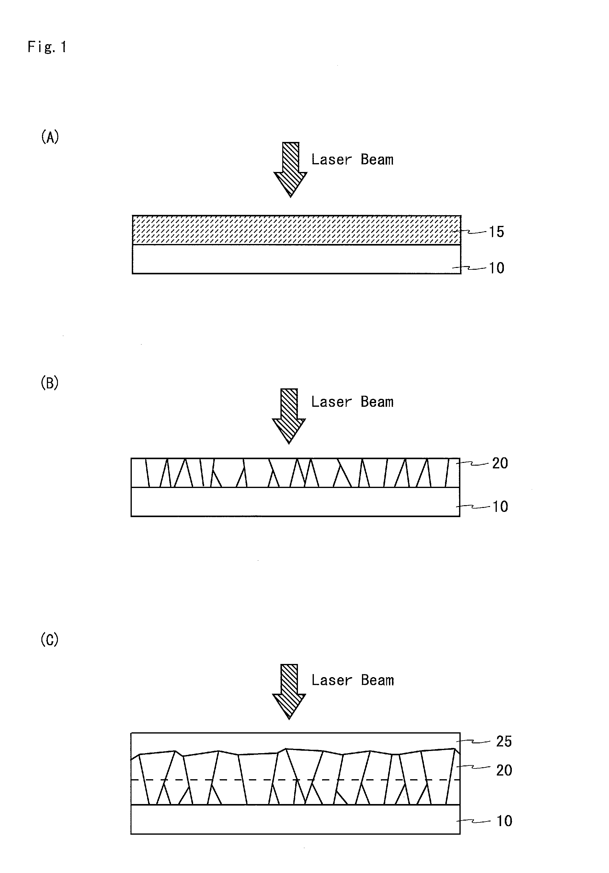
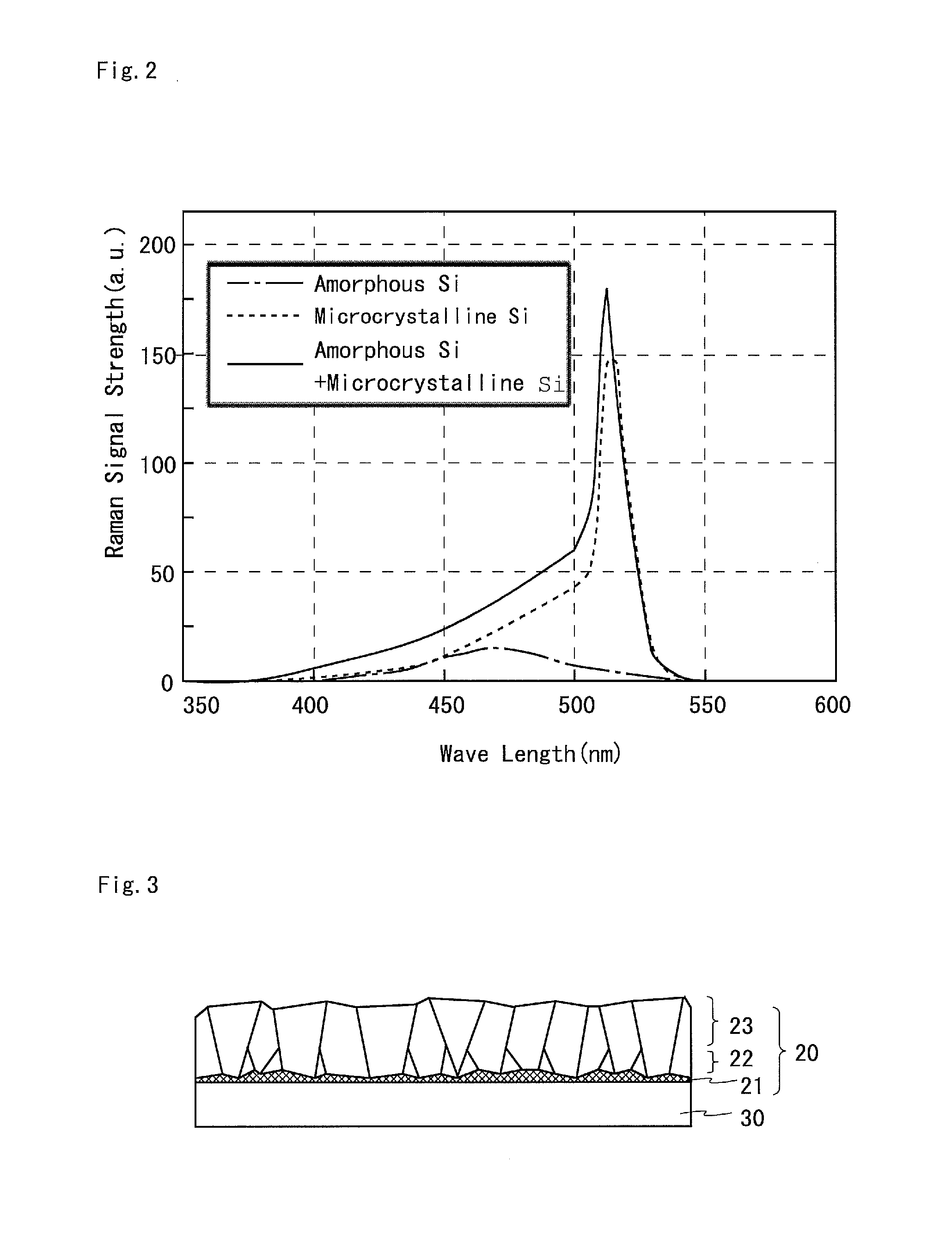
[0084]FIG. 5(A) is a sectional view showing a configuration of the TFT 100 according to the first embodiment of the present invention wher...

second embodiment

3. Second Embodiment

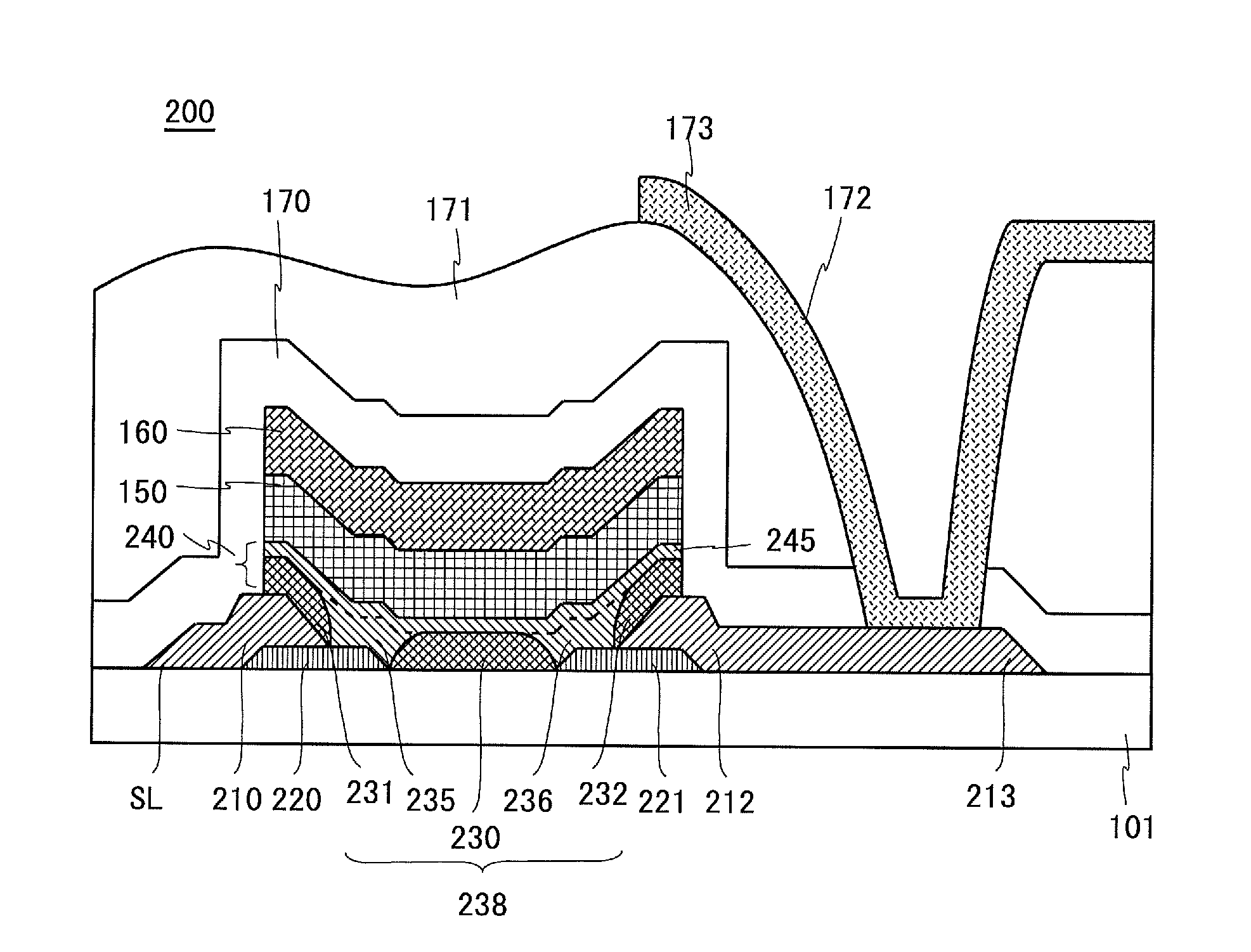
[0112]FIG. 11 is a sectional view showing a configuration of a TFT 200 according to a second embodiment of the present invention. Among the constituent elements of the TFT 200, the same elements as those found in the TFT 100 according to the first embodiment shown in FIG. 5(A) will be indicated with the same reference symbols. The description hereinafter will focus primarily on different constituent elements.

[0113]As shown in FIG. 11, on an insulated substrate provided by a glass substrate 101, n-type silicon layers (also will be called impurity-doped semiconductor layers) 220, 221 made of microcrystalline silicon and having tapered side surfaces are disposed at a predetermined distance from each other. The n-type silicon layer 220 has an exposed end on the side opposing to the n-type silicon layer 221, and an end covered by a source electrode 210. Also, the n-type silicon layer 221 has an exposed end on the side opposing to the n-type silicon layer 220, and an e...

third embodiment

4. Third Embodiment

[0126]FIG. 14 is a sectional view showing a configuration of a TFT 300 according to a third embodiment of the present invention. Among the constituent elements of the TFT 300, the same elements as those found in the TFT 200 according to the second embodiment shown in FIG. 11 will be indicated with the same reference symbols, and the description hereinafter will focus primarily on different constituent elements.

[0127]As shown in FIG. 14, two n-type silicon layers (also will be called impurity-doped semiconductor layers) 320, 321 of microcrystalline silicon which have tapered side surfaces are opposed to each other on a glass substrate 101. The n-type silicon layer 320 has an exposed end on a side opposed to the n-type silicon layer 321 whereas another end is flush with an end of the image signal lines SL, being different from the TFT 200. The n-type silicon layer 321 has an exposed end on the side opposed to the n-type silicon layer 320 whereas another end is flush...


PUM

PropertyMeasurementUnit
thicknessaaaaaaaaaa
thicknessaaaaaaaaaa
thicknessaaaaaaaaaa

Abstract

The present invention aims at reducing an OFF current in a thin film transistor while maintaining an ON-state current.
A TFT (100) includes a glass substrate (101) formed thereon with a source electrode (110) and a drain electrode (112) having their respective upper surfaces formed with n-type silicon layers (120, 121) of microcrystalline silicon. Microcrystalline silicon regions (135, 136) are formed respectively on the n-type silicon layers (120, 121) while an amorphous silicon region (130) is formed on the glass substrate (101), and these are covered by a microcrystalline silicon layer (145). Therefore, ON-state current flows from the drain electrode (112), through the microcrystalline silicon region (135), the microcrystalline silicon layer (145) and the microcrystalline silicon region (136) in this order, and then to the source electrode (110). Also, OFF current is limited by the amorphous silicon region (130).

Description

TECHNICAL FIELD[0001]The present invention relates to a thin film transistor and a method for manufacturing the same. More specifically, the present invention relates to a thin film transistor suitable for switching elements in pixel formation portions on a display panel or constituent elements of a drive circuit thereof, and to a method for manufacturing the thin film transistor.BACKGROUND ART[0002]In conventional active matrix liquid crystal display devices, thin film transistors (hereinafter called “TFT”) are utilized as switching elements in pixel formation portions. In recent years, however, TFT has been used not only as switching elements in pixel formation portions but also as elements for drive circuits, even in liquid crystal display devices manufactured from large substrates of newer generations including the sixth generation substrates, in an effort to reduce the manufacturing cost. In this trend, development has been made for changing the TFT's channel layers from conven...

Claims


Application Information

Patent Timeline
Patent Type & Authority Applications(United States)
IPC IPC(8): H01L29/786H01L21/336
CPCH01L29/04H01L29/66757H01L29/78696H01L29/78675H01L29/78609
Inventor NAKATANI, YOSHIKIMORIGUCHI, MASAOKANZAKI, YOHSUKETAKANISHI, YUDAI
Owner SHARP KK
Why Eureka
Try Eureka