Semiconductor device with buried gates and buried bit lines and method for fabricating the same

a technology of semiconductor devices and bit lines, which is applied in the direction of semiconductor devices, basic electric elements, electrical appliances, etc., can solve the problems of high probability of self-alignment contact failure of storage node contact, inability to perform masking, and inability to achieve masking. the effect of reducing the resistance of the bit lin

Inactive Publication Date: 2011-05-05
SK HYNIX INC
View PDF6 Cites 19 Cited by
  • Summary
  • Abstract
  • Description
  • Claims
  • Application Information

AI Technical Summary

Benefits of technology

[0012]An embodiment of the present invention is directed to a semiconductor device which may reduce the resistance of a bit line and prevent a bridging between a bit line and a storage node contact, and a method for fabricating the semiconductor device.

Problems solved by technology

First, when the bit line contact hole 18A is formed for high integration, the size of the contact hole should be formed small. In this case, when the contact hole is formed too small, the contact hole may not be opened, which is called a contact-hole-not-open phenomenon. In this case, it may be impossible to perform a mask process.
Second, when the bit line 18 is formed, a process of forming a nitride spacer 18B, which surrounds the bit line 18, needs to be performed to prevent a short from occurring between the storage node contact 19 and the bit line 18. With the nitride spacer forming process performed additionally, the cross-sectional area of a bit line may be reduced so as to increase resistance.
Third, since the bit line 18 is positioned in the upper portion of the active region 13, the connection portion with the active region 13 may become weak when a storage node contact hole for the storage node contact 19.
Fourth, the over-lay margins of the bit line 18 and the bit line contact hole 18A are so poor that the bit line 18 and the bit line contact hole 18A may be bridged with an adjacent storage node contact and thus a self-alignment contact failure of the storage node contact is highly likely to occur.

Method used


Image

  • Semiconductor device with buried gates and buried bit lines and method for fabricating the same
  • Semiconductor device with buried gates and buried bit lines and method for fabricating the same
  • Semiconductor device with buried gates and buried bit lines and method for fabricating the same

Examples


first embodiment

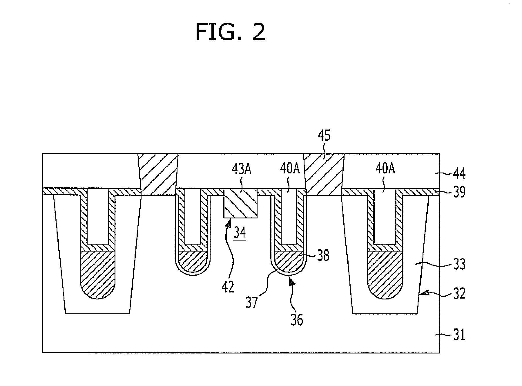
[0032]FIG. 2 is a cross-sectional view illustrating the semiconductor device fabricated in accordance with the present invention.

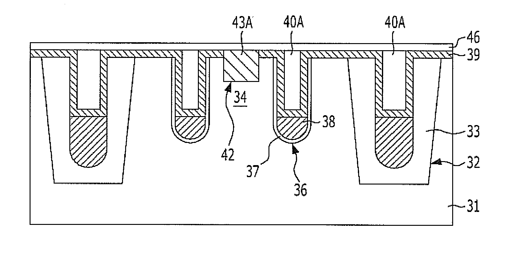
[0033]Referring to FIG. 2, the semiconductor device includes a plurality of first trenches 36 formed in the inside of an active region 34, a buried gate 38 filling a portion of the inside of an individual first trench 36, a second trench 42 formed in the inside of the active region 34 between buried gates 38, and a buried bit line 43A filling the second trench 42. The semiconductor device also includes storage node contacts 45 formed at both ends of the active region 34 to penetrate an inter-layer dielectric layer 44.

[0034]Each active region 34 is defined by an isolation layer 33 over a substrate 31, and the active region 34 has a shape of island slanted in an oblique direction. The isolation layer 33 is formed to fill an isolation trench 32 through a Shallow Trench Isolation (STI) process.

[0035]The buried gate 38 and the buried bit line 43A are formed cro...

second embodiment

[0057]FIG. 3I is a cross-sectional view illustrating buried bit lines formed in accordance with the present invention. According to the structure shown in FIG. 3I, when the buried bit line 43A is a copper layer, a copper diffusion barrier 46 is additionally formed over the substrate structure including the buried bit line 43A. The other constituent elements except the copper diffusion barrier 46 are the same as shown in FIG. 3G.

[0058]Cells are laid out in the types of FIGS. 4A and 4B in order to form buried gates and buried bit lines in accordance with the first and second embodiments of the present invention.

[0059]FIGS. 4A and 4B are layouts of the semiconductor devices in accordance with the first and second embodiments of the present invention, respectively.

[0060]Referring to FIG. 4A, when the active regions 34 are formed in the shape of a linear island, the buried gate 38 and the buried bit line 43A are not crossed perpendicularly, but the angle between the buried gate 38 and th...

third embodiment

[0063]FIG. 5 is a cross-sectional view illustrating the semiconductor device fabricated in accordance with the present invention.

[0064]Referring to FIG. 5, the semiconductor device includes a plurality of first trenches 66 formed in the inside of an active region 64, a buried gate 68 filling a portion of the inside of an individual first trench 66, a second trench 72 formed to be extended in a direction crossing the buried gates 68, a third trench 75 formed in a direction crossing the second trench 72 between buried gates 68, and a buried bit line 76A filling the third trench 75 and the second trench 72. The semiconductor device also includes storage node contacts 80 formed at both ends of the active region 64 to penetrate a second inter-layer dielectric layer 79.

[0065]Each active region 64 is defined by an isolation layer 63 over a substrate 61, and the active region 64 has a shape of island slanted in an oblique direction. The isolation layer 63 is formed to fill an isolation tren...


PUM


Abstract

A semiconductor device includes: a plurality of first trenches formed inside a plurality of active regions; a plurality of buried gates configured to partially fill insides of the plurality of the first trenches; a plurality of second trenches formed to be extended in a direction crossing the plurality of the buried gates; and a plurality of buried bit lines configured to fill the plurality of the second trenches.

Description

CROSS-REFERENCES TO RELATED APPLICATIONS[0001]The present application claims priority of Korean Patent Application Nos. 10-2009-0104626 and 10-2009-0104641, both filed on Oct. 30, 2009, which are incorporated herein by reference in their entirety.BACKGROUND OF THE INVENTION[0002]Exemplary embodiments of the present invention relate to a method for fabricating a semiconductor device, and more particularly, to a semiconductor device with buried gates and buried bit lines, and a method for fabricating the semiconductor device.[0003]Recently, semiconductor device fabrication processes are being developed to have an increased degree of integration. Among diverse methods for securing reliability and integration degree of a semiconductor device is a method of using buried gates. The parasitic capacitance between a gate and a bit line can be remarkably reduced by burying the gate in the inside of an active region. The gate buried in the inside of an active region is referred to as a buried ...

Claims


Application Information

Patent Timeline
Patent Type & Authority Applications(United States)
IPC IPC(8): H01L29/78H01L21/28
CPCH01L21/743H01L27/10885H01L27/10876H01L27/0207H10B12/053H10B12/482
Inventor KIM, SU-YOUNG
Owner SK HYNIX INC
Why Eureka
Try Eureka