Electronic device suitable for bioimplantation

Active Publication Date: 2011-05-05
KONINKLIJKE PHILIPS ELECTRONICS NV
View PDF15 Cites 5 Cited by
  • Summary
  • Abstract
  • Description
  • Claims
  • Application Information

AI Technical Summary

Benefits of technology

[0004]The object is achieved according to the invention by providing an electronic device suitable for bioimplantation, comprising: at least one rechargeable power source, at least electronic component connected to said power source, and magnetoelectric conversion means connected to said power source to enable recharging of said power source, said magnetoelectric conversion means comprising a stack of at least one magnetoelastic layer and at least one piezoelectric layer, wherein said magnetoelectric conversion means has a three-dimensional geometry for receiving and magnetoelectrically converting a magnetic field originating from multiple directions respectively. The substantially improved efficiency of the electronic device is firstly due to the application of said magnetoelectric stack (laminate) of said at least one magnetoelastic layer and said at least one piezoelectric layer, preferably a stack of at least one piezoelectric layer which is sandwiched between multiple magnetoelastic layers, by means of which stack the magnetic field induced can be converted relatively efficiently into electrical energy. In case said stack is subjected to an (alternating) magnetic field the magnetoelastic layer and consequently the piezoelectric layer will be deformed resulting in the generation of an electrical current within the piezoelectric layer. The induced electrical current is subsequently used to (re)charge the power source of the electronic device. The term “magnetoelectric” thus refers to the effect in which an electric current is produced in a laminate when it is subjected to a magnetic field. The term “piezoelectric” refers to the effect in those materials which only produce an electric output when they experience a change in mechanical load. The substantially improved efficiency of the electronic device according to the invention is secondly due to the improved degree of freedom of design of the magnetoelectric conversion means, and hence of the electronic device as such, which degree of freedom is many times larger than this freedom offered by the state of the art. Due to this freedom of design the magnetoelectric conversion means is easily provided a three-dimensional geometry for receiving and magnetoelectrically converting a magnetic field originating from multiple directions respectively. In this context the term “three-dimensional geometry” implies the application of a magnetoelectric stack provided with a three-dimensional shape such that an improved probability can be obtained that at least a part of said stack is oriented substantially perpendicular to (a component of) the applied magnetic field, in order to secure the generation of sufficient electrical energy to charge the power source of the electronic device according to the invention. The risk of depletion of all electrical energy that can be provided by the power source due to (too) poor charging of the power source can thus be counteracted this way. In case the electronic device is implanted in a body cavity, the electronic device can either be fixedly attached to the body or can, to a certain extent, be freely moveably within said body cavity. Although the electronic device according to the invention will commonly be used as bioimplantable device, it would also be conceivable to apply the electronic device in other applications, for example in water treatment plants or in chemical engineering equipment such as a chemical reactors, pipelines, et cetera.
[0005]Suitable materials to be utilized as the magnetoelastic material in a magnetoelastic sensor may be any material with a non-zero magnetostriction and a high magnetoelastic coupling, such as iron-nickel alloys, rare earth metals, ferrites, such as spinel type ferrites (Fe3O4, MnFe2O4), silicon-iron alloys, many other different alloys and mixtures thereof. Soft magnetoelastic materials, alloys

Problems solved by technology

During the twentieth century, energy consumption increased dramatically and an unbalanced energy management exists.
These devices need power supplies that will operate for extremely long durations as maintenance would necessitate surgery.
The restriction makes the application of a flat (2D) rectangular or circular coil design rather inefficient.
Moreover, this restriction implies that a electronic device with a

Method used


Image

  • Electronic device suitable for bioimplantation
  • Electronic device suitable for bioimplantation
  • Electronic device suitable for bioimplantation

Examples


Embodiment Construction

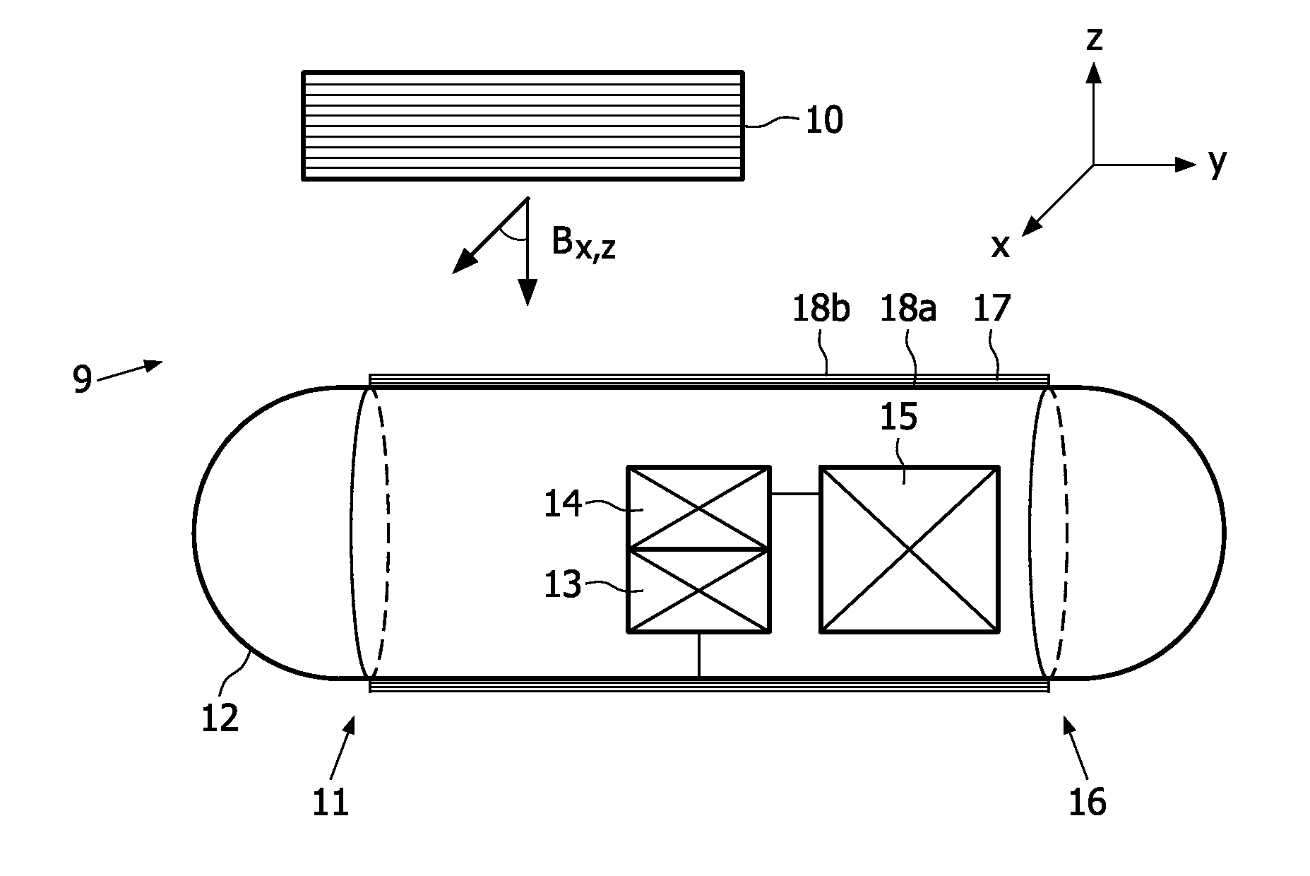
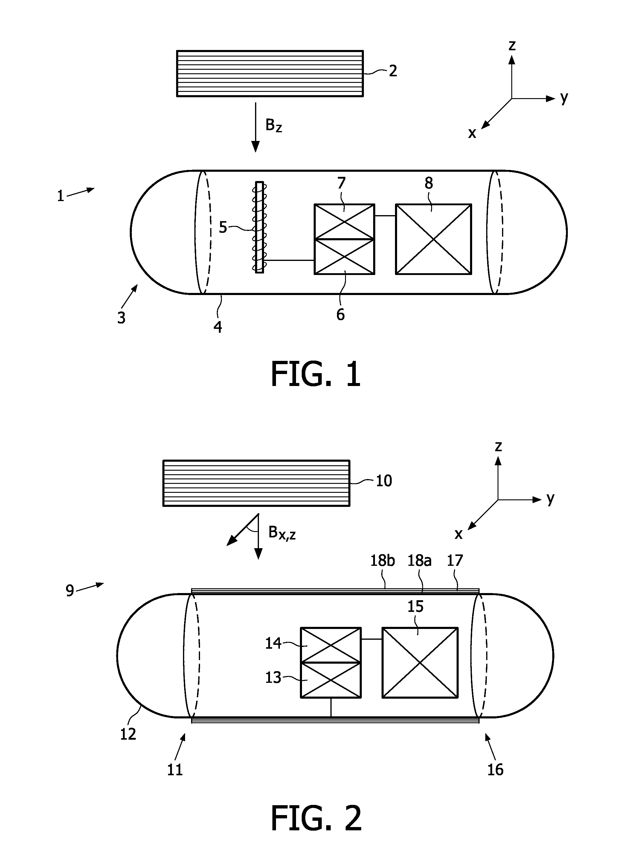
[0015]FIG. 1 shows a schematic cross section of an assembly 1 of a magnetic charging unit 2 and a bioimplantable electronic device 3 known from the prior art. The known device 3 comprises a cylindrical pill shaped housing 4 enclosing a coil 5, a power management system 6 connected to said coil 5, a rechargeable battery 7 connected to said power management system 6, and an electronic component 8, such as a sensor, connected to said battery 7. By means of the charging unit 2 an alternating magnetic field B is imposed to the electronic device 3. The coil 5 will convert the magnetic field B into electrical energy which is used to (re)charge the battery 7. A first drawback of the known device 3 is that by means of the coil 5 merely a relatively poor and inefficient transfer of energy within the device 3 can be achieved. Moreover, the coil 5 is substantially sensitive for a magnetic field Bz which is perpendicular to each winding of the coil 5. In case the magnetic field would originate f...


PUM


Abstract

The present application discloses an integrated circuit comprising a circuit portion (100) coupled between first and second power supply lines (110; 120); a first switch (115, 135) coupled between the first power supply line (110, 120) and the circuit portion (100) for disconnecting the circuit portion from the first power supply line during an inactive mode of the circuit portion; and an arrangement (315, 335, 410) for, during said inactive mode, providing the circuit portion (100) with a fraction of its active mode power supply at least when averaged over said inactive mode to prevent the circuit portion voltage to drop below a threshold value. The present application further discloses a method for controlling such an integrated circuit.

Description

FIELD OF THE INVENTION[0001]The invention relates to an electronic device suitable for bioimplantation. The invention also relates to an assembly of an electronic device according to the invention and a charging unit adapted to generate a magnetic field.BACKGROUND OF THE INVENTION[0002]During the twentieth century, energy consumption increased dramatically and an unbalanced energy management exists. While there is no sign that this growth in demand will abate (particularly amongst the developing nations), there is now an awareness of the transience of non-renewable resources and the irreversible damage caused to the environment. In addition, there is a trend towards the miniaturization and portability of computing and communications devices. These energy-demanding applications require small, light power sources that are able to sustain operation over long periods of time, particularly in remote locations such as space and exploration. Furthermore, advances in medical science are lea...

Claims


Application Information

Patent Timeline
IPC IPC(8): H02J7/00H01L41/22H01L41/39H01L41/45
CPCA61N1/3787H01M10/425Y02E60/12H01M10/46H01M10/44Y02E60/10
Inventor NIESSEN, ROGIER ADRIANUS HENRICAPASVEER, WILLEM FRANKE
Owner KONINKLIJKE PHILIPS ELECTRONICS NV
Why Eureka
Try Eureka