Liquid crystal display device driving method and liquid crystal display device

a technology of liquid crystal display device and driving method, which is applied in static indicating device, non-linear optics, instruments, etc., can solve the problems of insufficient shortening the time required for spray-bend transition, and not taking into account the spray-bend transition in the conventional structur

Inactive Publication Date: 2011-05-05
SHARP KK
View PDF13 Cites 5 Cited by
  • Summary
  • Abstract
  • Description
  • Claims
  • Application Information

AI Technical Summary

Benefits of technology

[0079]As such, it is possible to provide a method of driving a liquid crystal display device that makes it possible to cause the spray-bend transition all over the display surface in a short period of time, in a liquid crystal display device including a plurality of pixel electrodes.

Problems solved by technology

However, the conventional structure has not taken into consideration a spray-bend transition that spreads beyond a bus line such as a gate bus line.
This causes a problem that the time required for the spray-bend transition was not sufficiently shortened.

Method used


Image

  • Liquid crystal display device driving method and liquid crystal display device
  • Liquid crystal display device driving method and liquid crystal display device
  • Liquid crystal display device driving method and liquid crystal display device

Examples


embodiment 1

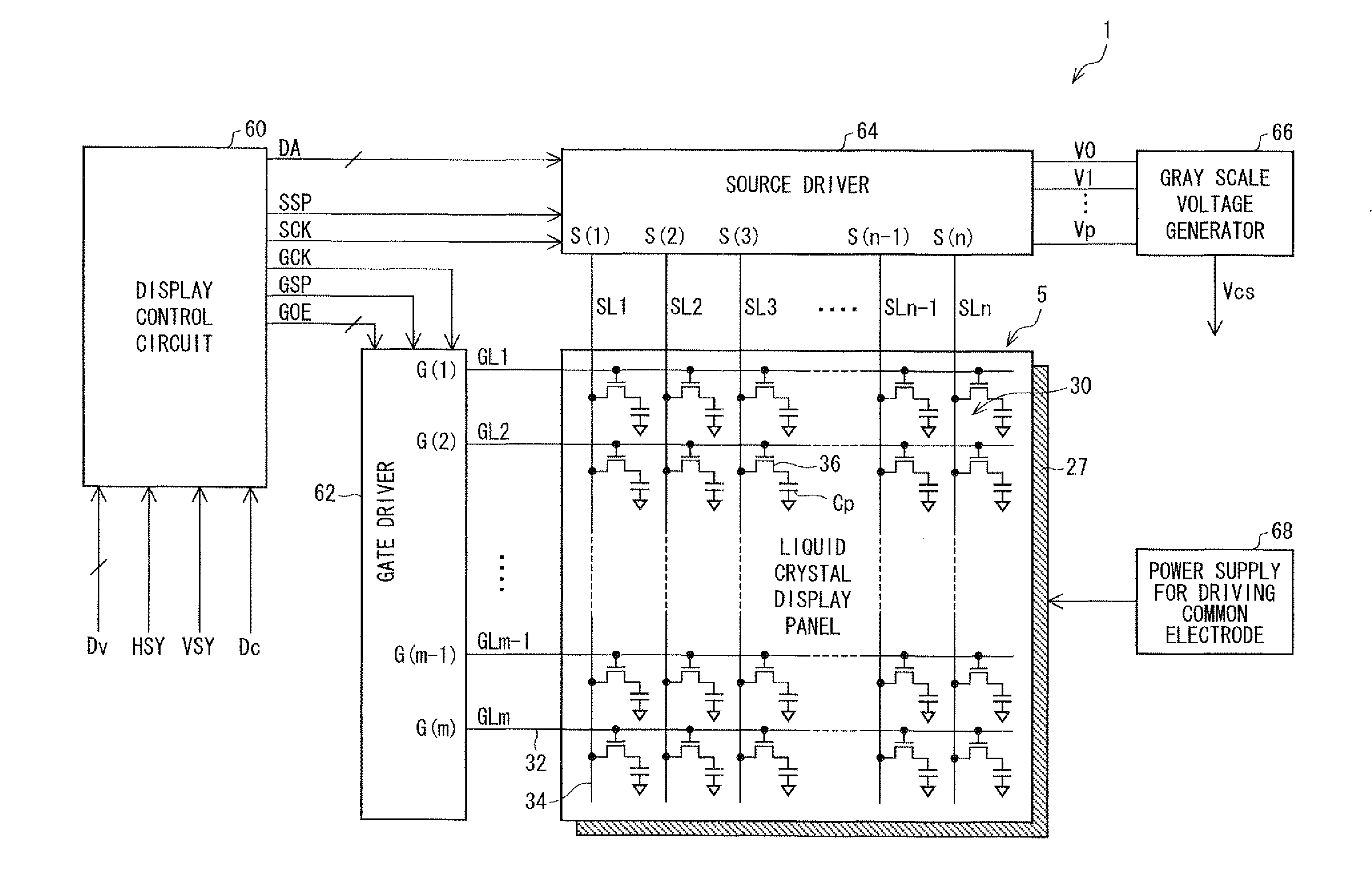
[0113]A first embodiment of the present invention is described with reference to FIGS. 1 through 3. FIG. 1 is a block diagram schematically illustrating how a liquid crystal display device 1 is arranged.

[0114]The liquid crystal display device 1 of the present embodiment includes: a gate driver 62 serving as a scanning signal line driving circuit; a source driver 64 serving as a data signal line driving circuit; a display control circuit 60 which controls the gate driver 62 and the source driver 64; a gray scale voltage generator 66; a power supply for driving counter electrode 68 for driving a counter electrode 27; and an active matrix type (TFT type) liquid crystal display panel 5.

[0115]The liquid crystal display panel 5 in the liquid crystal display device 1 includes: gate bus lines 32 (GL1 through GLm) serving as a plurality of scanning signal lines (m scanning signal lines); source bus lines 34 (SL1 through SLn) serving as a plurality of data signal lines (n data signal lines) w...

embodiment 2

[0167]Next, a second embodiment of the present invention is described. It should be noted that structures that are not described in the present embodiment are the same as those described in Embodiment 1. Further, members that have the same functions as those illustrated in figures referred to in Embodiment 1 are given the same reference numerals as those illustrated in the figures, and descriptions of the members are omitted, for convenience of description.

[0168](Data Signal Line Serving as Source Bus Line)

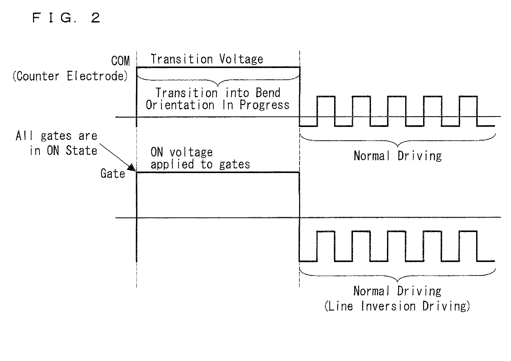
[0169]In a liquid crystal display panel 5 in which pixels 30 are provided in a matrix manner, in a case where an identical data voltage (an identical data signal) is applied to all the source bus lines 34 when all the gate bus lines 32 are simultaneously put into the ON state, then the identical data voltage is to be written to all the pixels 30 of the liquid crystal display panel 5. Accordingly, it is possible to achieve a state where all the pixel electrodes 17 have an identical...

embodiment 3

[0172]Next, a third embodiment of the present invention is described. It should be noted that structures that are not described in the present embodiment are the same as those described in Embodiments 1 and 2. Further, members that have the same functions as those illustrated in figures referred to in Embodiments 1 and 2 are given the same reference numerals as those illustrated in the figures, and descriptions of the members are omitted, for convenience of description.

[0173]Unlike the liquid crystal display devices 1 described in Embodiments 1 and 2, a liquid crystal display device 1 of the present embodiment is characterized in that, in the line sequential driving, occurrence of a lateral electrical field is prevented by preventing an electric potential difference between any adjacent pixel electrodes 17 between which a corresponding one of gate bus lines 32 is provided.

[0174](Waveform of Signal Applied to Storage Capacitor Electrode)

[0175]That is, according to a liquid crystal di...


PUM

PropertyMeasurementUnit
voltageaaaaaaaaaa
dielectric anisotropyaaaaaaaaaa
electric potentialaaaaaaaaaa

Abstract

The present invention is characterized in that: switching elements are transistor elements (36); a plurality of gate bus lines (32) and a plurality of source bus lines are provided on an active matrix substrate (10) in a lattice manner; each of the transistor elements (36) is connected to at least one of the gate bus lines (32) and at least one of the source bus lines; and a period is secured during which no electric potential difference occurs between any adjacent ones of the plurality of pixel electrodes (17) between which a corresponding one of the plurality of gate bus lines (32) is provided, at least while a transition voltage for causing a transition of the liquid crystal molecules into the bend orientation state is being applied to the liquid crystal layer, by simultaneously putting all of the plurality of gate bus lines (32) into an ON state so that voltages of identical polarity are applied to the respective any adjacent ones of the plurality of pixel electrodes (17).

Description

TECHNICAL FIELD[0001]The present invention relates to a method of driving a liquid crystal display device, and a liquid crystal display device. The present invention particularly relates to an OCB (Optically Self-Compensated Birefringence) mode liquid crystal display panel and an OCB mode liquid crystal display device.BACKGROUND ART[0002]A liquid crystal display device has the advantages that it (i) is thinner and lighter than a CRT (Cathode Ray Tube) display device and (ii) consumes less electric power than the CRT (Cathode Ray Tube) display device because the liquid crystal display device can be driven by a lower voltage than the CRT (Cathode Ray Tube) display device. Therefore, the liquid crystal display device has been used in a variety of electronic devices such as a television set, a laptop computer (personal computer), a desktop personal computer, a PDA (personal digital assistant, i.e., a mobile terminal), and a mobile phone.[0003]Meanwhile, an electronic device, such as a l...

Claims


Application Information

Patent Timeline
Patent Type & Authority Applications(United States)
IPC IPC(8): G02F1/136
CPCG02F1/1395G09G2310/063G09G2300/0491G09G3/3648
Inventor KATAYAMA, TAKASHISHIMIZU, MASAHIRO
Owner SHARP KK
Why Eureka
Try Eureka