Optical sensor

Inactive Publication Date: 2007-05-17
NAT INST OF ADVANCED IND SCI & TECH
View PDF4 Cites 27 Cited by
  • Summary
  • Abstract
  • Description
  • Claims
  • Application Information

AI Technical Summary

Benefits of technology

[0022] The present invention has the aforementioned configuration. It is, therefore, possible to provide

Problems solved by technology

It is, therefore, difficult to produce such the optical sensors, and the optimum conditions such as doping conditions etc. are limited within narrow ranges.
Eventually, there has been a problem that the yield is low, and the cost is high.
Further, since the background-art semiconductor optical sensors are manufactured by epitaxial growth in which the range of selection as to materials is limited, there is another problem that

Method used


Image

  • Optical sensor
  • Optical sensor
  • Optical sensor

Examples


Example

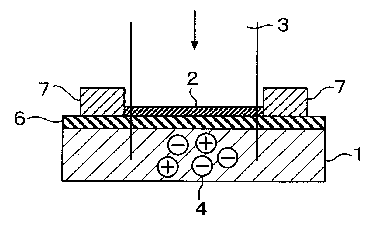
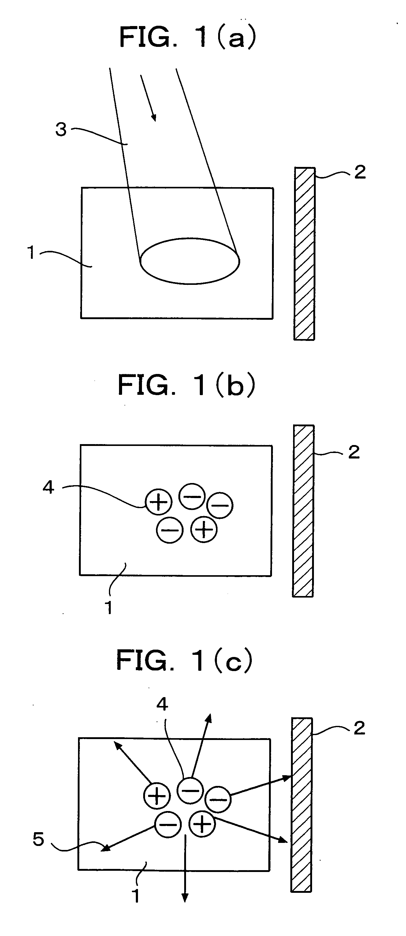
[0043]FIG. 2 and FIG. 3 are views for explaining the first embodiment of the present invention. FIG. 2 is a perspective view of an optical sensor, and FIG. 3 is a sectional view of the optical sensor.

[0044] As shown in these drawings, a carbon nanotube 2 is formed on a photoconductive material 1 through an insulating layer 6, and electrodes 7 and 7 for applying an appropriate voltage are provided in the opposite ends of the carbon nanotube 2.

[0045] In the case of this embodiment, a silicon substrate (photoconductive material 1) having photoconductivity is used, the insulating layer 6 of silicon oxide is formed thereon, and the carbon nanotube 2 is disposed thereon.

[0046] The photoconductive material 1 may be produced by crystal growth with a vacuum evaporation apparatus such as a molecular beam epitaxy apparatus (MBE apparatus), or a chemical vapor deposition apparatus (CVD apparatus) such as a metal-organic chemical vapor deposition apparatus (MOCVD) . The photoconductive materi...

Example

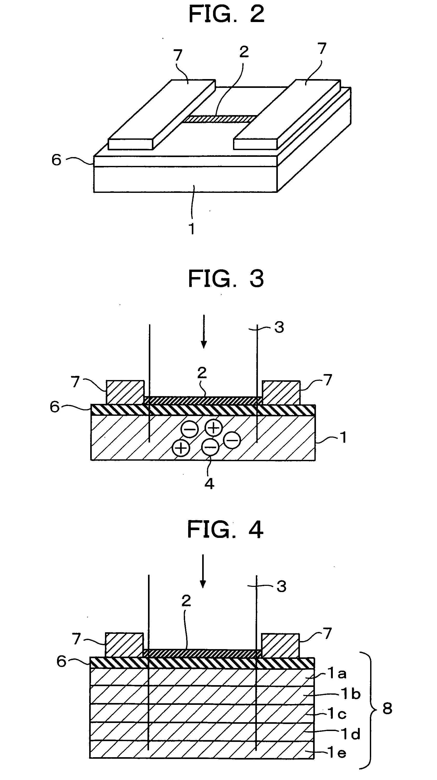
[0048]FIG. 4 is a sectional view of an optical sensor for explaining the second embodiment of the present invention. This embodiment uses a multilayer structure 8 of a plurality of kinds of photoconductive materials 1a to 1e having photoconductivity in different wavelength ranges. In such a manner, it is possible to produce an optical sensor having sensitivity all over the photosensitive wavelength ranges of the respective photoconductive materials 1.

[0049] The photosensitive wavelength ranges in the photoconductive materials 1 will be shown below by way of example. Silicon (Si) ranges over 200-1,100 nm; germanium (Ge), 500-1,500 nm; gallium arsenide (GaAs), 200-900 nm; indium gallium arsenide (InGaAs), 650-2,900 nm; and indium arsenide (InAs), 1,300-3,900 nm.

[0050] Innumerable combinations can be set, for example, using aluminum arsenide (AlAs), aluminum gallium arsenide (AlGaAs), indium aluminum arsenide (InAlAs), gallium arsenide phosphide (GaAsP), indium gallium arsenide phosp...

Example

[0054]FIG. 5 is a sectional view of an optical sensor for explaining the third embodiment of the present invention. In this embodiment, a gate electrode 9 is provided under a photoconductive material 1 so as to form a field effect transistor structure.


PUM


Abstract

An optical sensor is characterized by comprising a photoconductive material (1) which generates a carrier (4) inside when irradiated with a light or an electromagnetic wave (3), and carbon nanotube (2), and by sensing the carrier (4), which is generated within the photoconductive material (1) by irradiation of the light or electromagnetic wave (3), through change of electrical conduction of the carbon nanotube (2).

Description

TECHNICAL FIELD [0001] The present invention relates to an optical sensor in which a photoconductive material or photoconductive materials are combined with a carbon nanotube or carbon nanotubes. BACKGROUND ART [0002] Generally, optical sensors are to convert energy of light or electromagnetic waves into electric energy. Background-art optical sensors include photodiodes, avalanche photodiodes, phototransistors, photo-MOSs, CCD sensors and CMOS sensors having semiconductor as their main components, photomultiplier tubes using photoelectric effect, etc. [0003] Of the former semiconductor optical sensors, some are to extract output signal as electric current by converting carriers into the external electric current directly, where the carriers are electron or positive holes generated by irradiation with light. Others are to extract output signal as a modulation of majority electric-current, where the modulation is formed by a local electric field by the photo-generated carriers accumu...

Claims


Application Information

Patent Timeline
IPC IPC(8): H01L31/113H01L27/30H01L31/0203H01L31/0232H01L31/08H01L31/09H01L31/112H01L51/00H01L51/30
CPCB82Y10/00H01L27/307H01L31/0203H01L31/0232H01L31/08H01L31/09H01L31/112H01L31/113H01L51/0048H01L51/0052H01L51/424H01L51/428H01L2224/48091H01L2224/73265H01L2924/00014Y02E10/549Y10S977/932Y10S977/954H01L31/02325H10K39/32H10K85/221H10K85/615H10K30/20H10K30/65
Inventor NAGAMUNE, YASUSHIMATSUMOTO, KAZUHIKO
Owner NAT INST OF ADVANCED IND SCI & TECH
Why Eureka
Try Eureka