Magnetoresistive memory with a wiring for suppressing crosstalk

a magnetic memory and wiring technology, applied in the field of magnetic memory with a wiring for suppressing crosstalk, can solve the problems of insufficient suppression of crosstalk, limit of impedance matching of conventional word lines, etc., and achieve the effect of suppressing crosstalk, efficiently applying magnetic field, and suppressing leakage magnetic field

Inactive Publication Date: 2004-08-17
PANASONIC CORP
View PDF10 Cites 29 Cited by
  • Summary
  • Abstract
  • Description
  • Claims
  • Application Information

AI Technical Summary

Benefits of technology

The present invention easily can provide the impedance matching of a pulse transmission line, thus decreasing a delay coefficient and suppressing the distortion of a pulse waveform. Therefore, a high-speed response can be achieved in a MRAM. Moreover, the present invention can make the coupling between adjacent word lines relatively weak, so that crosstalk in the MRAM can be reduced easily.
XMnSb (X represents a metallic element, preferably at least one selected from Ni, Pt, Pd and Cu) can provide a large MR ratio because of its high magnetic polarizability.

Problems solved by technology

However, there is a limit to impedance matching of the conventional word line, and crosstalk cannot be suppressed sufficiently.

Method used


Image

  • Magnetoresistive memory with a wiring for suppressing crosstalk
  • Magnetoresistive memory with a wiring for suppressing crosstalk
  • Magnetoresistive memory with a wiring for suppressing crosstalk

Examples


example 1

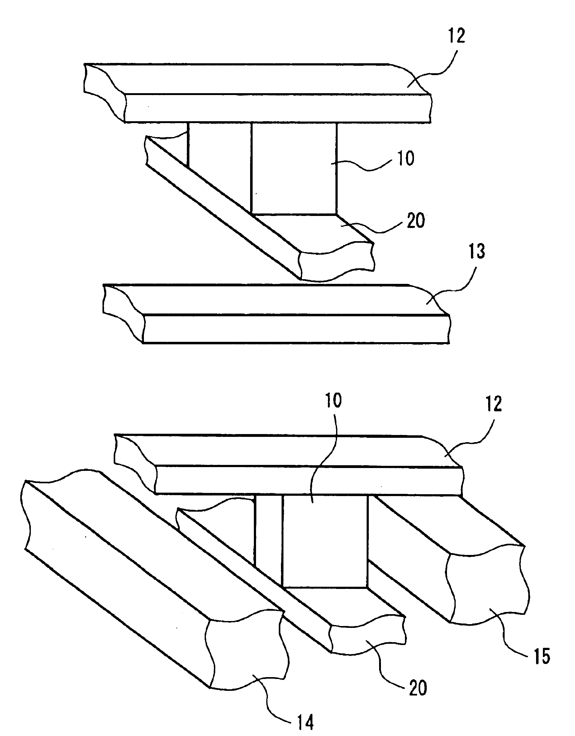
Using a multi-target sputtering apparatus, a MR element with the multi-layer structure shown in FIG. 19F was produced. This MR element has the following film configuration:

Ni.sub.0.81 Fe.sub.0.19 (2) / Ru(0.7) / Ni.sub.0.81 Fe.sub.0.19 (3) / Al.sub.2 O.sub.3 (1.2) / Cu.sub.0.75 Fe.sub.0.25 (2) / Ru(0.7) / CO.sub.0.75 Fe.sub.0.25 (2) / PtMn(20).

Here, the films are arranged in the order mentioned from the top to the bottom of the element, and the figures in parentheses denote the film thickness (nm).

This example uses two types of Al.sub.2 O.sub.3 layer, each of which serves as a tunnel insulating layer. The type A was prepared by forming an Al film with sputtering and oxidizing the Al film. The type B was prepared by depositing Al.sub.2 O.sub.3 itself with sputtering. The type A was oxidized in any one of the following manners: natural oxidation in a vacuum vessel, natural oxidation in a vacuum vessel with increased temperature, and oxygen-containing plasma oxidation in a vacuum vessel. In either c...

example 2

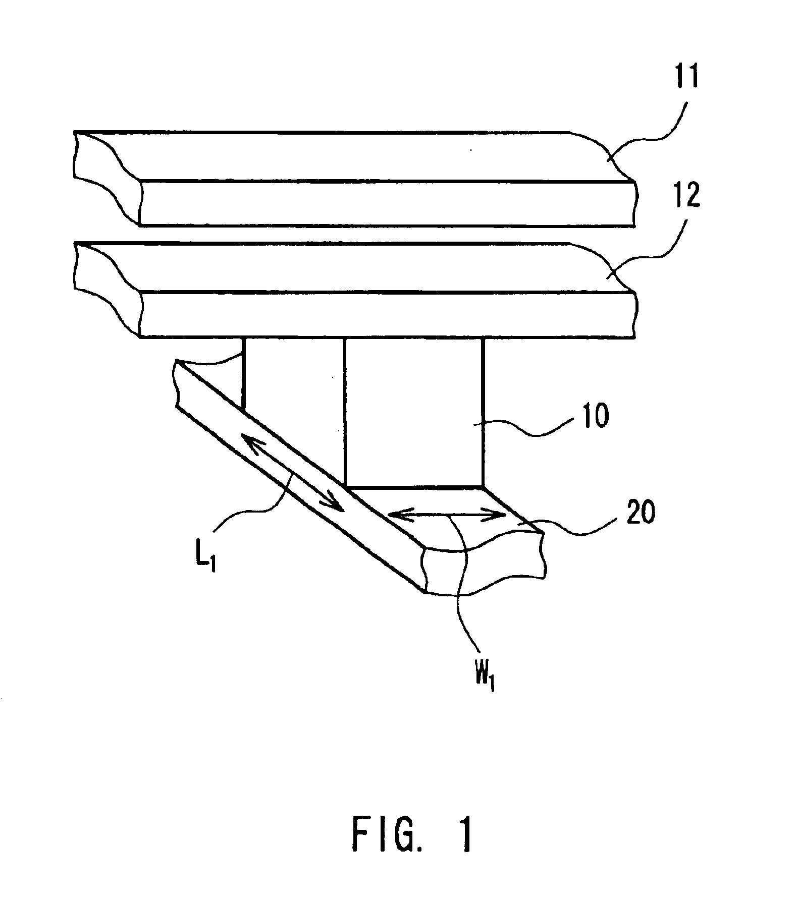
MRAMs that differ in the arrangement of word lines as shown in FIGS. 20A to 20F were produced in the same manner as Example 1. The word line included a signal line 91 and passive lines 92, 93. The passive line 92 and the signal line 91 sandwiched a MR element (not shown), and the passive line 93 and the signal line 91 were formed in the same plane. In FIGS. 20A to 20F, the signal line and the MR element have one-to-one correspondence.

Both the signal line 91 and the passive line 92 had a width of 0.2 .mu.m. In each of the MRAMs, the distance between a lower ground plane 100 and the closest conductive wires 91 to 93 was 100 .mu.m, and the distance between an upper ground plane (not shown) and the signal line 91 was 100 .mu.m.

A population of 1000 samples for each of the MRAMs was evaluated based on the malfunction of unselected memories that were adjacent to the word line through which signals constituting one word were sent. Table 1 shows the results. In Table 1, d represents a space ...

example 3

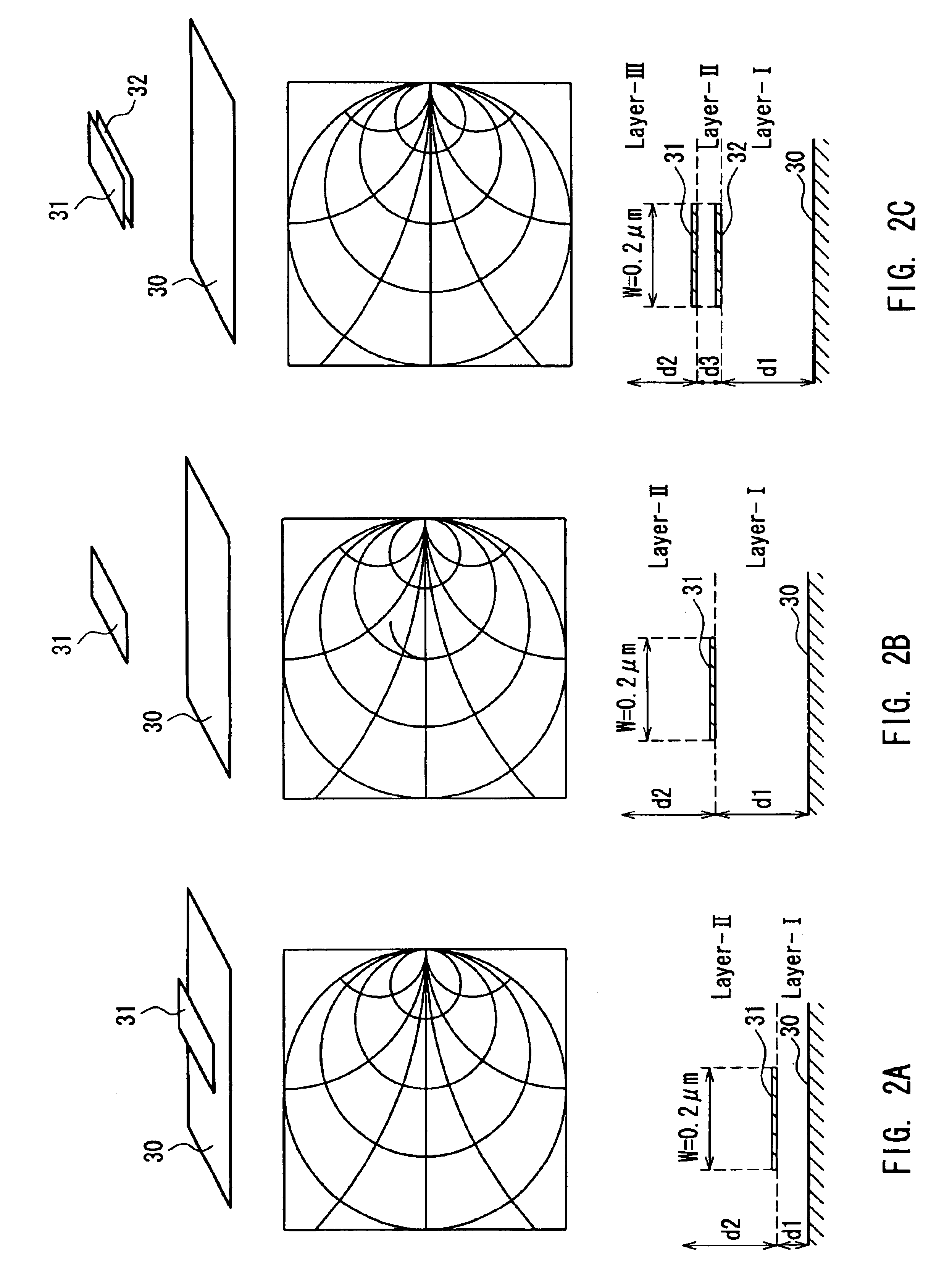
A MRAM was produced in the same manner as Example 1. In this example, the MRAM included a conductive wire 33 between adjacent MR elements other than a pair of conductive wires 31, 32, as shown in FIG. 8D.

The transmission of a pulse signal to the word lines 31 to 33 was evaluated with the MRAM. Each of the word lines had a width of about 0.5 .mu.m and a thickness of about 0.3 .mu.m, and the distance between the adjacent word lines was about 0.3 .mu.m. The terminal resistance was connected to either end of the wiring, and the characteristic impedance was adjusted to about 75 .OMEGA..

Under the input conditions that the time required for the applied pulse to rise from 1V to 5V was 1 ns and the transmission time (the length of the wiring was about 10 cm) was 0.5 ns, it took the signal 1 ns to rise. Compared with a single word line, the signal was not reflected significantly at the near end and the far end of the word lines when viewed from the pulse sending side.

Next, the effect of cross...


PUM


Abstract

A magnetoresistve memory device includes a magnetoresistive element and a wiring for applying a magnetic field to the magnetoresistive element. The wiring includes two or more conductive wires that extend in the same direction. A plurality of conductive wires is used to apply a magnetic field to a single magnetoresistive element, thereby achieving high-speed response and suppressing crosstalk.

Description

The present invention relates to a magnetoresistive memory device that utilizes a magnetoresistance effect. In particular, the present invention relates to a magnetoresistive memory device suitable for high-speed pulse transmission.A magnetic random access memory (MRAM) has been studied as a solid-state memory device including magnetoresistive elements (MR elements). The MRAM is provided with a conductive wiring that includes word lines and sense lines: the word lines are used to generate a magnetic field that is applied to the MR elements for recording and the sense lines are used for reading. A conventional MRAM uses a NiFe film or the like that has an anisotropic magnetoresistance (AMR) effect, expressed by a magnetoresistance ratio (MR ratio) of about 2%. However, it is difficult to increase the output of this MRAM. Ever since an artificial lattice film, in which magnetic films are exchange-coupled via a non-magnetic film, was proved to exhibit a giant magnetoresistance (GMR) ef...

Claims


Application Information

Patent Timeline
Patent Type & Authority Patents(United States)
IPC IPC(8): G11C11/15G11C11/02G11C11/14G11C11/16H01L21/8246H01L27/22H01L43/08
CPCB82Y10/00G11C11/14G11C11/15G11C11/16H01L27/228H01L43/08G11C11/1659G11C11/161G11C11/1675H10B61/22H10N50/10
Inventor ODAGAWA, AKIHIROHIRAMOTO, MASAYOSHIMATSUKAWA, NOZOMU
Owner PANASONIC CORP
Why Eureka
Try Eureka