Surface mount footprint in-line capacitance

a capacitance and footprint technology, applied in the field of surface mount footprint in-line capacitance, can solve the problems of reducing the integrity with which signals are propagated, high frequency system, and general size of electronic systems, and achieve the effect of improving signal integrity and routability

Active Publication Date: 2011-05-05
AMPHENOL CORP
View PDF10 Cites 85 Cited by
  • Summary
  • Abstract
  • Description
  • Claims
  • Application Information

AI Technical Summary

Benefits of technology

[0008]The inventors have recognized and appreciated that for electrical interconnection systems in which electronic components, such as capacitors, are connected in signal paths, improved signal integrity and routability may be achieved by incorporating the capacitors within the footprint of a surface mount electrical connector. One end of each capacitor may be connected to a shared conductive mounting pad on a printed circuit board (PCB) that is also used for attaching a contact tail of a conductive element of the electrical connector to the PCB. A second end of each capacitor may be attached to a second conductive mounting pad containing a via, as would conventionally exist in a mounting pad in an electrical connector footprint. The capacitor spans the shared mounting pad and the second mounting pad, connecting the conductive element of the connector to a trace within the printed circuit board through the capacitor.

Problems solved by technology

Electronic systems have generally become smaller, faster and functionally more complex.
Unfortunately, the via creates a disruption in the uniform impedance of the microstrip transmission line and therefore diminishes the integrity with which signals are propagated.
Capacitors block the flow of low frequency signals, which, in a high frequency system, may be noise.

Method used


Image

  • Surface mount footprint in-line capacitance
  • Surface mount footprint in-line capacitance
  • Surface mount footprint in-line capacitance

Examples


Embodiment Construction

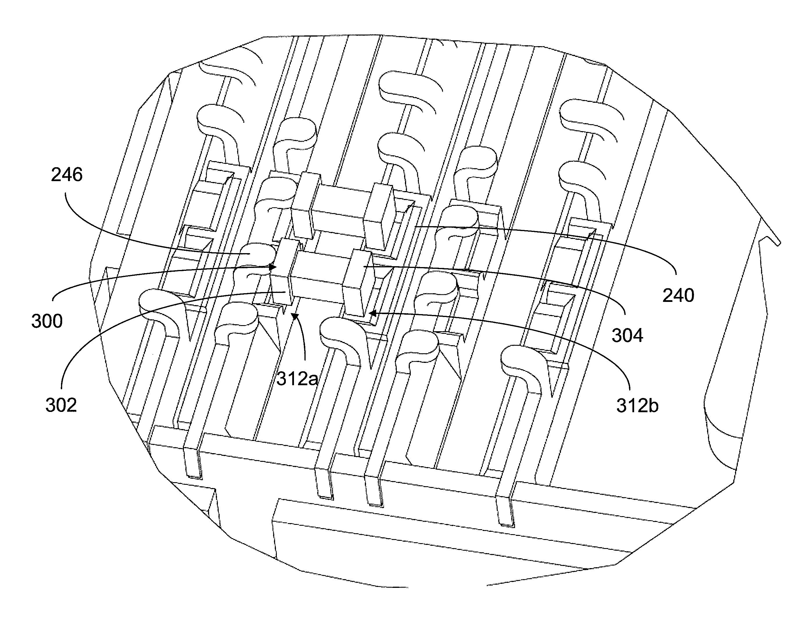
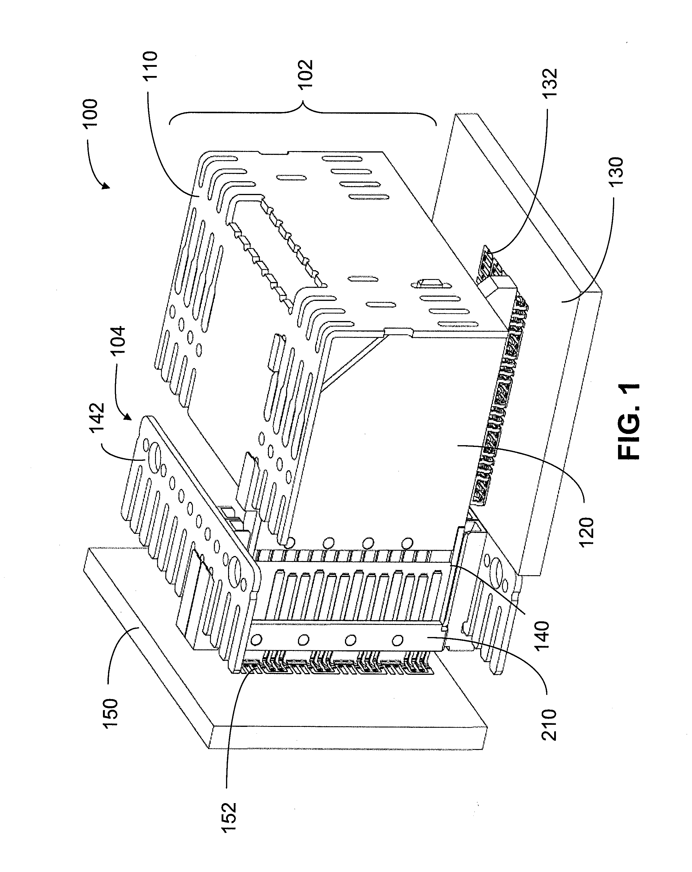
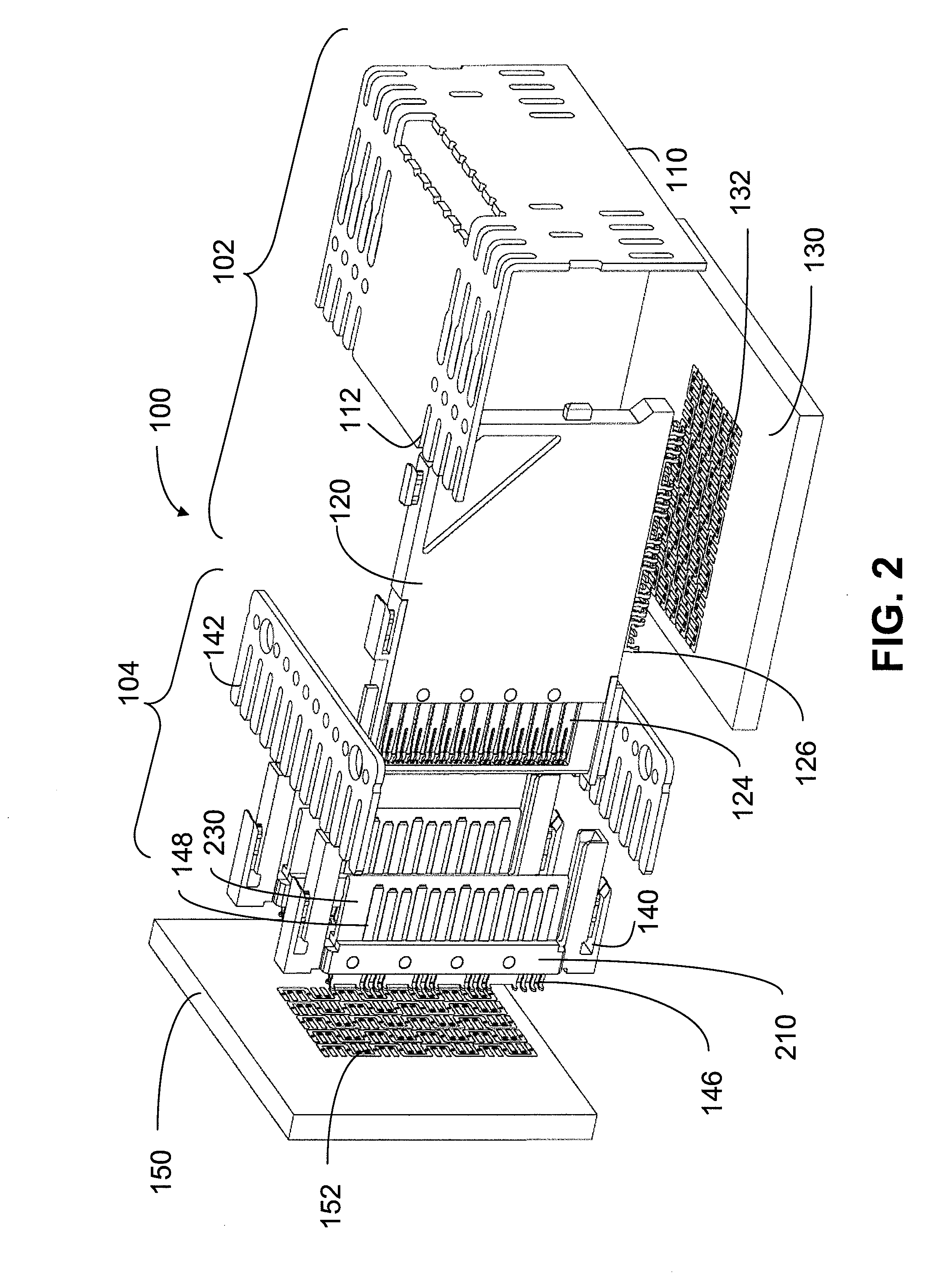
[0030]The inventors have recognized and appreciated that an improved electronic interconnection system may be formed by placing electronic components, described as capacitors in exemplary embodiments herein, on conductive pads of a substrate, described as a PCB in illustrative embodiments herein, that are within the footprint of a component, described as an electrical connector in illustrative embodiments herein, to be mounted to the PCB. Ends of the capacitors may be connected to pads within the footprint for establishing electrical pathways between signal conductors within the connector and the PCB, which is described in exemplary embodiments as a backplane, but may be a daughter card or other suitable substrate.

[0031]A footprint on the PCB may have mounting pads positioned where contact tails of signal conductors within the connector may be suitably connected to the PCB. However, not all mounting pads may be in direct connection with a via in the PCB. The footprint pattern may al...


PUM

PropertyMeasurementUnit
center-to-center distanceaaaaaaaaaa
lengthaaaaaaaaaa
lengthaaaaaaaaaa

Abstract

An interconnection system with capacitors integrated into a printed circuit board footprint of an electrical connector. One end of each capacitor shares a pad on the printed circuit board with a contact tail of a conductive element in a connector. The shared pads are not connected through vias to internal circuit structures. Rather, a via, such as which would conventionally be formed as part of the connector mounting pad, is formed as part of a separate, adjacent pad. A second end of the capacitor is attached to the adjacent pad, forming an electrical connection between the conductive element and the via through the capacitor. Incorporating capacitors into the footprint reduces the number of vias required, which improves signal integrity. The capacitors may be placed on the printed circuit board separately from the connector or may be incorporated into the connector, allowing the connector and capacitors to be placed in one operation.

Description

BACKGROUND[0001]This invention relates generally to electrical interconnections for connecting printed circuit boards.[0002]Electrical connectors are used in many electronic systems. It is generally easier and more cost effective to manufacture a system on several printed circuit boards (“PCBs”) that are connected to one another by electrical connectors than to manufacture a system as a single assembly. A traditional arrangement for interconnecting several PCBs is to have one PCB serve as a backplane. Other PCBs, which are called daughter boards or daughter cards, are then connected through the backplane by electrical connectors.[0003]Electronic systems have generally become smaller, faster and functionally more complex. These changes mean that the number of circuits in a given area of an electronic system, along with the frequencies at which the circuits operate, have increased significantly in recent years. Current systems pass more data between printed circuit boards and require ...

Claims


Application Information

Patent Timeline
Patent Type & Authority Applications(United States)
IPC IPC(8): H01R13/66H05K7/02H05K3/34H05K1/11H05K1/16
CPCH01R13/6466Y10T29/49144H05K3/34H01R13/6587
Inventor GIRARD, JR., DONALD A.GAILUS, MARK W.STOKOE, PHILIP T.
Owner AMPHENOL CORP
Why Eureka
Try Eureka