Plasma processing apparatus

a processing apparatus and plasma technology, applied in the direction of coatings, chemical vapor deposition coatings, electric discharge tubes, etc., can solve the problems of deteriorating the uniformity of the generated plasma in the circumferential direction, local damage of the dielectric window existing between the coil and the plasma, and the current change along the path of the coil, so as to improve the uniformity of the generated plasma

Active Publication Date: 2011-05-12
HITACHI HIGH-TECH CORP
View PDF11 Cites 394 Cited by
  • Summary
  • Abstract
  • Description
  • Claims
  • Application Information

AI Technical Summary

Benefits of technology

[0018]The plasma processing apparatus of the present invention includes a conductor disposed near the induction antenna and arranged along the induction antenna, and the mutual inductances at circumferential positions between the conductor and induction antenna and between the conductor and plasma are controlled, so that it becomes possible to compensate for the coil current non-uniformity along the circumference of the coil, and to improve the uniformity of the generated plasma in the circumferential direction.

Problems solved by technology

The high voltage and stray capacitance cause the following two problems.
One problem is that the high voltage on the coil is electrostatically coupled with the plasma via the stray capacitance existing between the induction coil and the plasma, causing local damage of the dielectric window existing between the coil and the plasma.
The other problem is that while the current circulates through the coil, the stray capacitance existing in the path causes the coil current to change along the path deteriorating the uniformity of the generated plasma in the circumferential direction.
However, the method introducing the coupling capacitor disclosed above had the following problems.
One problem is that the coupling capacitor has an effect to suppressing the non-uniformity of the circulating current along the circumference, but cannot make perfectly the current uniform.
The second problem is that the optimum value of the capacitor must be varied according to operation conditions (operation plasma density, pressure, used gas conditions, etc.), but it is impossible to replace the capacitor corresponding to such various conditions in mass production apparatuses.
The attempt to adopt a variable capacitor as the capacitor causes increase of cost of the control unit and complication of operation methods.
The third problem is that the coupling capacitor must have a property to endure a few tens of KVA, according to which the geometrical shape of the capacitor is increased, and the attempt to mount the capacitor in a matching box disposed on the upper portion of the apparatus causes the matching box size to increase, leading to problems related to mounting design.

Method used


Image

  • Plasma processing apparatus
  • Plasma processing apparatus
  • Plasma processing apparatus

Examples


Embodiment Construction

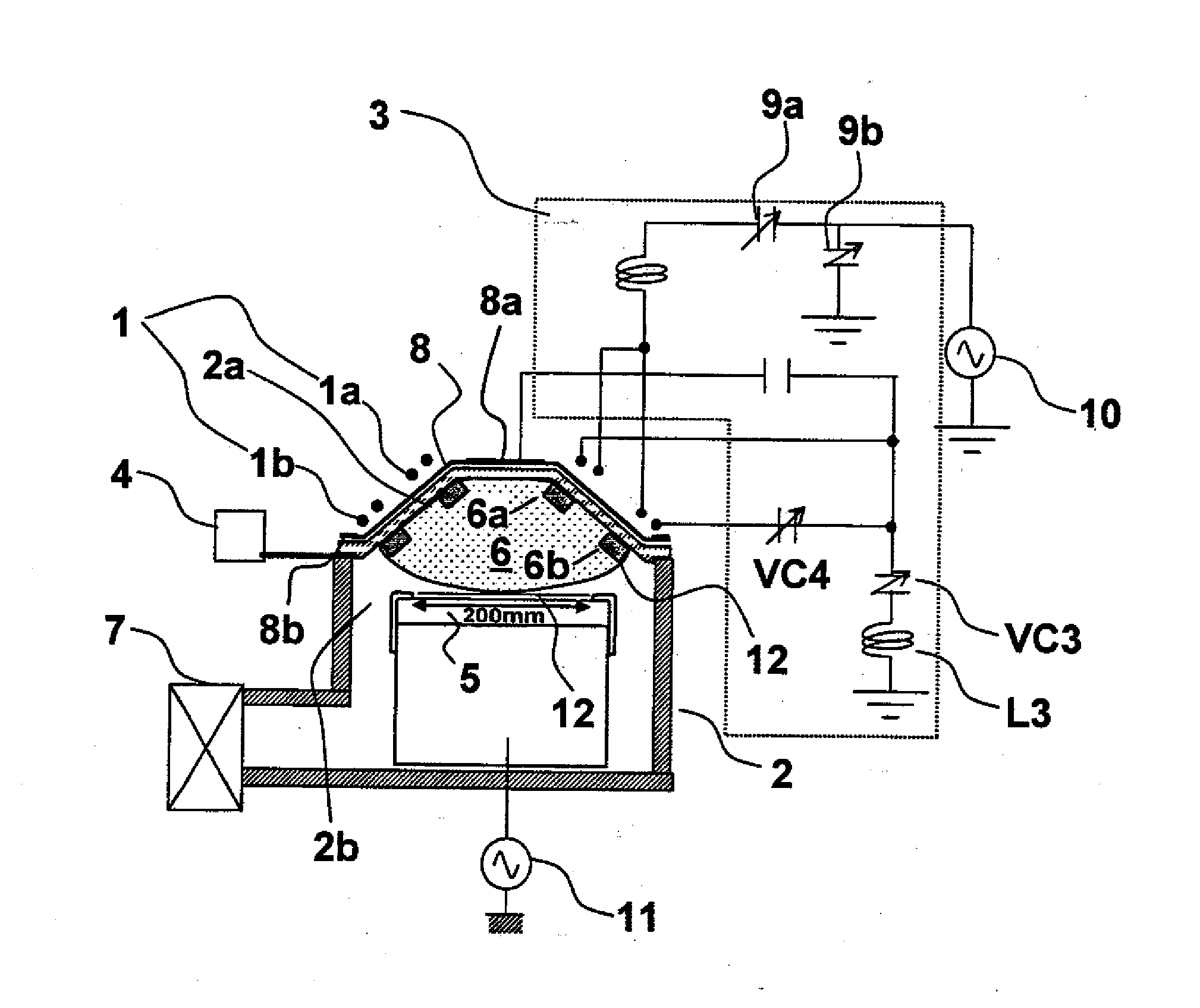
[0044]Now, the preferred embodiments of the plasma processing apparatus will be described with reference to the drawings.

[0045]A first preferred embodiment takes the inductively coupled etching apparatus disclosed in patent document 2 as an example, and the means to compensate non-uniform circulating coil current will now be described, taking the inductively coupled etching apparatus as an example.

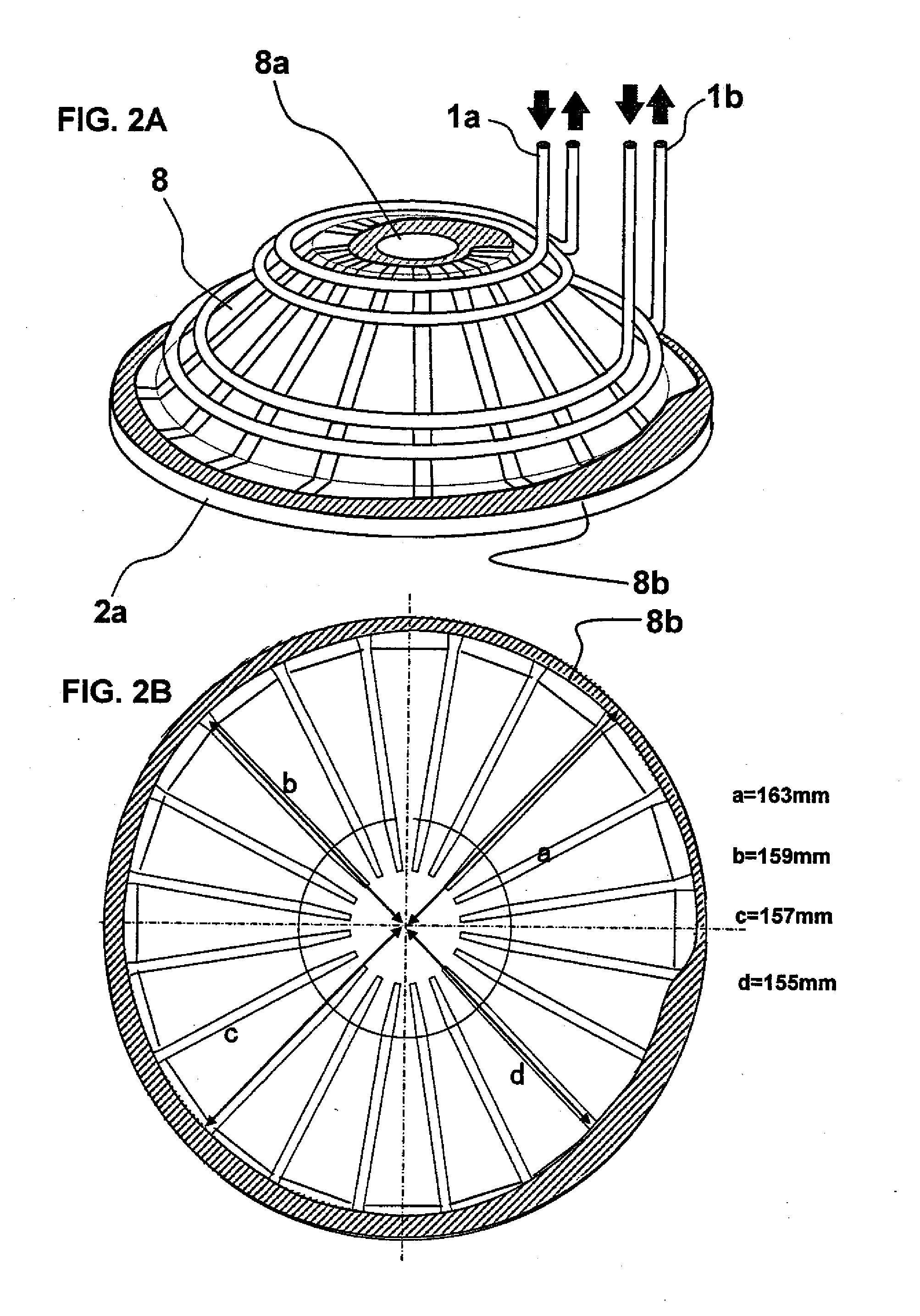
[0046]FIG. 1 is a cross-sectional view of a plasma processing apparatus according to the present invention. A vacuum chamber 2 includes a discharge window 2a composed of an insulating material forming a plasma generation portion (such as a nonconductive material like Al2O3 ceramics), and a processing unit 2b having an electrode 5 for placing a sample 12 which is the object to be processed. On the outer side of the discharge window 2a is disposed an inductively coupled antenna 1 having the form of a coil. The inductively coupled antenna 1 is respectively separated into two coil systems, a t...


PUM

PropertyMeasurementUnit
insulatingaaaaaaaaaa
areaaaaaaaaaaa
dielectricaaaaaaaaaa

Abstract

The invention provides a plasma processing apparatus in which ring-like conductors 8a and 8b are arranged closed to and along an induction antenna 1 composed of an inner circumference coil 1a and an outer circumference coil 1b. Ring-like conductors 8a and 8b are each characterized in that the radius from the center of the apparatus and the cross-sectional shape of the conductor body varies along the circumferential angle of the coils. Since the mutual inductances between the ring-like conductors 8a and 8b and the induction antenna 1 and between the ring-like conductors 8a and 8b and the plasma along the circumferential position are controlled, it becomes possible to compensate for the coil currents varied along the circumference of the coils of the induction antenna 1, and to improve the non-uniformity in the circumferential direction of the current in the generated plasma.

Description

[0001]The present application is based on and claims priority of Japanese patent application No. 2009-257312 filed on Nov. 10, 2009, the entire contents of which are hereby incorporated by reference.BACKGROUND OF THE INVENTION[0002]1. Field of the Invention[0003]The present invention relates to a plasma processing apparatus using plasma for performing surface processing such as etching a substrate or forming thin films on a substrate.[0004]2. Description of the Related Art[0005]In the field of manufacturing semiconductor devices, inductively-coupled plasma processing apparatuses are adopted as etching and CVD apparatuses. In inductively coupled plasma processing apparatuses, an induction coil formed of a few turns is disposed on the outer side of a vacuum chamber and high frequency current is supplied to the induction coil, to thereby feed power to the plasma generated in the vacuum chamber and maintain the generated plasma. In order to supply sufficient current through the inductio...

Claims


Application Information

Patent Timeline
Patent Type & Authority Applications(United States)
IPC IPC(8): C23F1/08C23C16/00
CPCH01J37/321H01J37/32623H01J37/3211
Inventor YOSHIOKA, KENYOSHIGAI, MOTOHIKONISHIO, RYOJIKAWAGUCHI, TADAYOSHI
Owner HITACHI HIGH-TECH CORP
Why Eureka
Try Eureka