Methods for fabricating trench metal oxide semiconductor field effect transistors

a technology of trench metal oxide and semiconductor field effect, which is applied in the direction of transistors, semiconductor devices, electrical equipment, etc., can solve the problems that the gate charge in the trench mosfet may limit the high speed (or dv/dt) application, and achieve the enhancement of gate conductivity the reduction of poly sheet resistance of the cellular trench mosfet, and the effect of improving the robustness of the gate conductor structur

Inactive Publication Date: 2011-05-12
O2 MICRO INC
View PDF20 Cites 3 Cited by
  • Summary
  • Abstract
  • Description
  • Claims
  • Application Information

AI Technical Summary

Benefits of technology

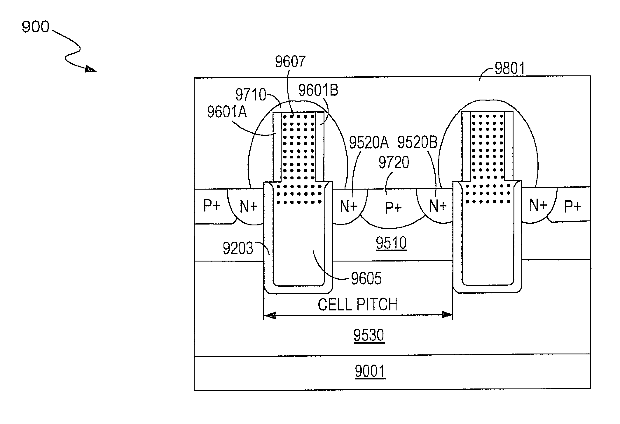
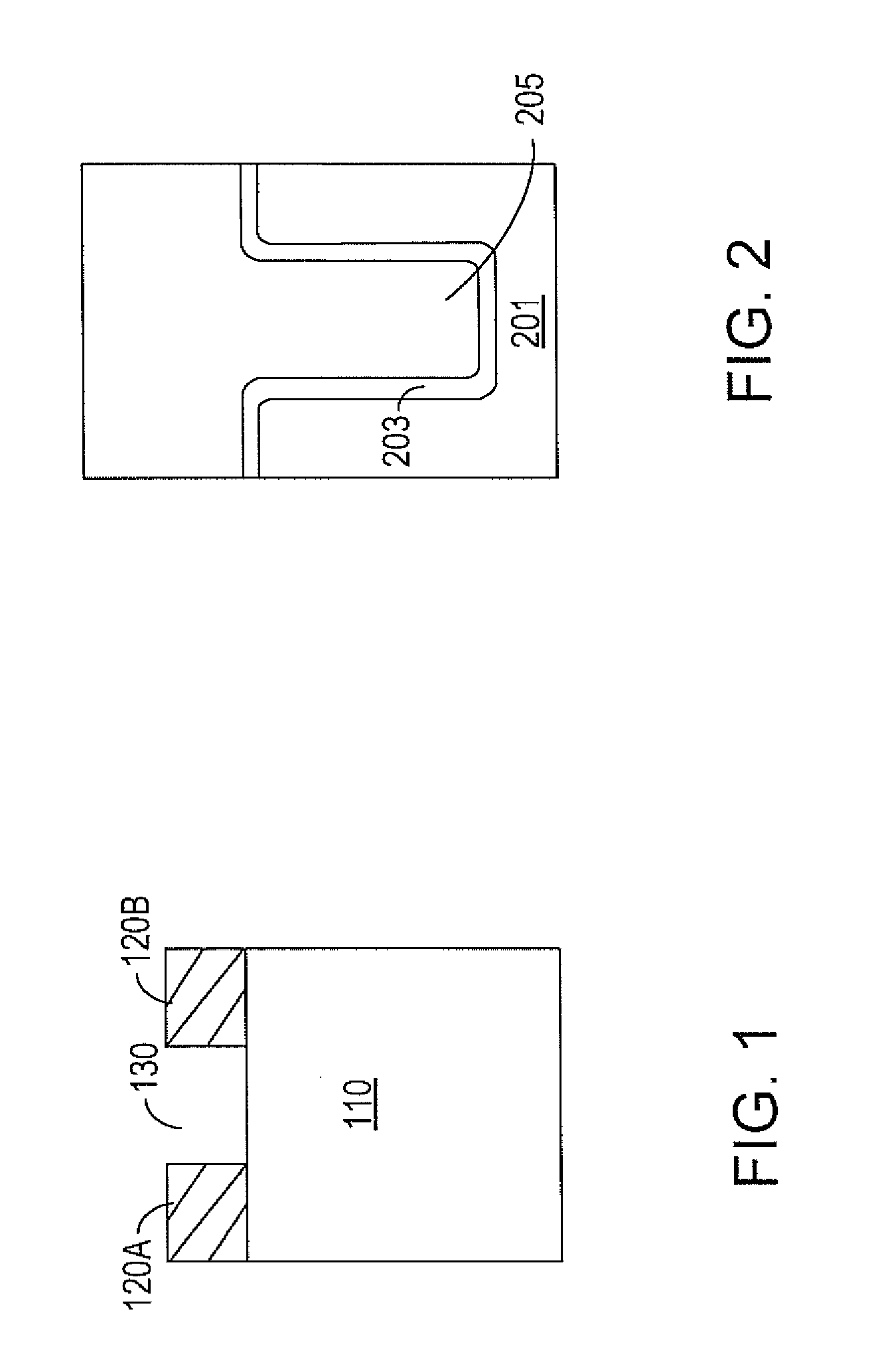
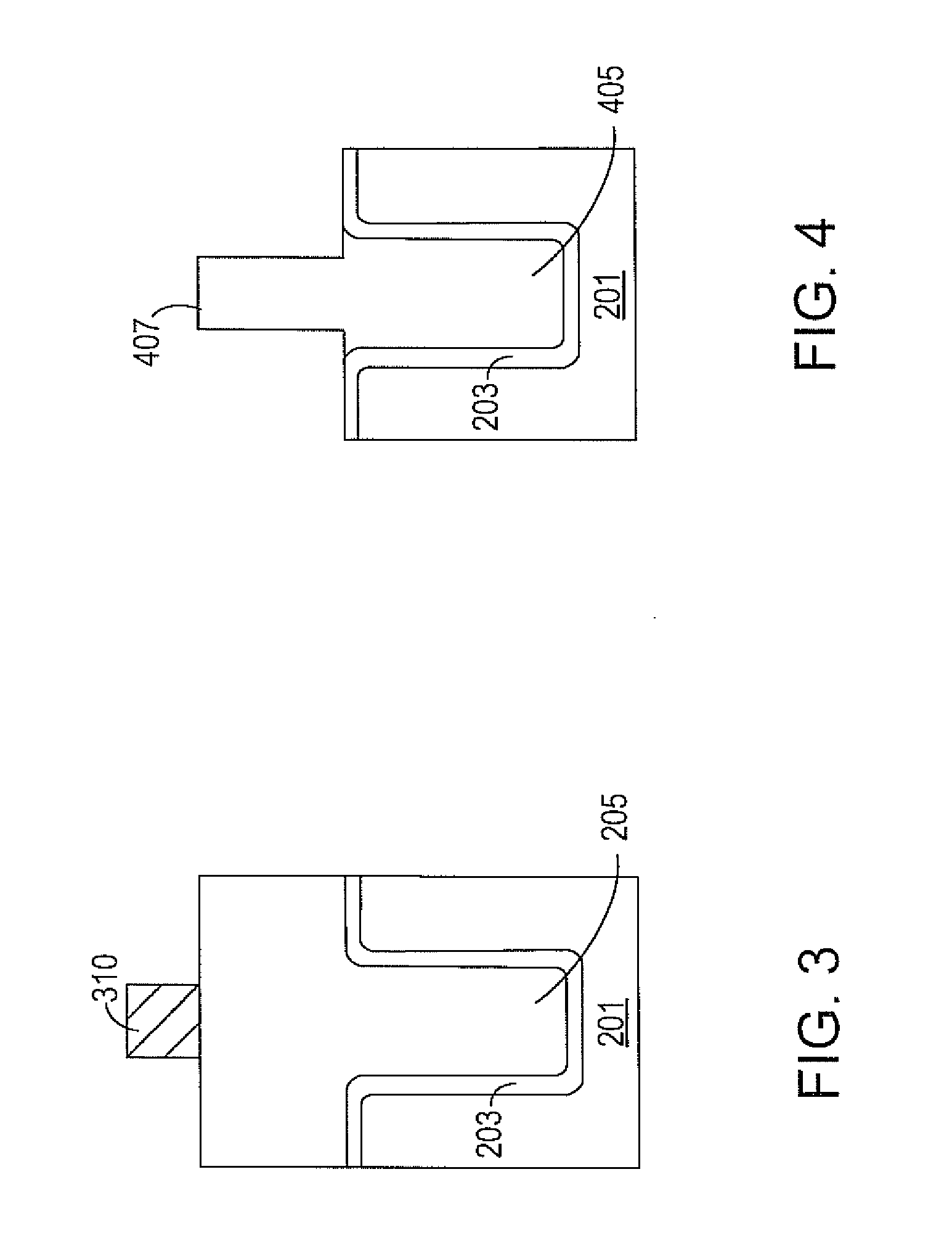
[0004]Embodiments of the invention pertain to methods for fabricating a cellular trench metal oxide semiconductor field effect transistor (MOSFET). In one embodiment, the method includes depositing a first photoresist atop a first epitaxial (epi) layer to pattern a trench area, depositing a second photoresist atop a first gate conductor layer to pattern a mesa area, etching away part of the first gate conductor layer in the mesa area to form a second gate conductor layer with a hump, and titanizing crystally the second gate conductor layer to form a Ti-gate conductor layer. Edges of the mesa area are aligned to edges of the trench area. Hence, approximately more than half of polysilicon in the second gate conductor layer is titanized crystally. The poly sheet resistance of the cellular trench MOSFET can be reduced, and thus the gate conductivity of the cellular trench MOSFET is enhanced. A spacer can be formed to protect corners of the first gate conductor layer and to make the gate conductor structure more robust for mechanical support.

Problems solved by technology

However, gate charges in the trench MOSFET may limit high speed (or dv / dt) applications compared to DVMOSFET.

Method used


Image

  • Methods for fabricating trench metal oxide semiconductor field effect transistors
  • Methods for fabricating trench metal oxide semiconductor field effect transistors
  • Methods for fabricating trench metal oxide semiconductor field effect transistors

Examples


Embodiment Construction

[0010]In the following detailed description of the present invention, numerous specific details are set forth in order to provide a thorough understanding of the present invention. However, it will be recognized by one skilled in the art that the present invention may be practiced without these specific details or with equivalents thereof. In other instances, well-known methods, procedures, components, and circuits have not been described in detail as not to unnecessarily obscure aspects of the present invention.

[0011]Some portions of the detailed descriptions that follow are presented in terms of procedures, logic blocks, processes, and other symbolic representations of operations for fabricating semiconductor devices. These descriptions and representations are the means used by those skilled in the art of semiconductor device fabrication to most effectively convey the substance of their work to others skilled in the art. In the present application, a procedure, logic block, proces...


PUM


Abstract

A method for fabricating a cellular trench metal oxide semiconductor field effect transistor (MOSFET) includes depositing a first photoresist atop a first epitaxial (epi) layer to pattern a trench area, depositing a second photoresist atop a first gate conductor layer to pattern a mesa area, etching away part of the first gate conductor layer in the mesa area to form a second gate conductor layer with a hump, and titanizing crystally the second gate conductor layer to form a Ti-gate conductor layer. Edges of the mesa area are aligned to edges of the trench area. Hence, approximately more than half of polysilicon in the second gate conductor layer is titanized crystally. A spacer can be formed to protect corners of the first gate conductor layer and to make the gate conductor structure more robust for mechanical support.

Description

RELATED APPLICATION[0001]This application claims priority to U.S. Provisional Application No. 61 / 259,275, titled “Methods for Fabricating Trench Metal Oxide Semiconductor Field Effect Transistor,” filed on Nov. 9, 2009, which is hereby incorporated by reference in its entirety.BACKGROUND[0002]During the past few decades, there has been an increasing interest in semiconductor devices, such as a power metal oxide semiconductor field effect transistor (MOSFET) used in various applications. The power MOSFET usually has a polysilicon layer. The polysilicon layer can be used, for example, as a gate electrode of the power MOSFET.[0003]The power MOSFET can have one of two major structures, e.g., a vertical diffused MOSFET (VDMOSFET) or a trench MOSFET. The VDMOSFET began available in the mid-1970s due to the availability of planar technology. By the late 1980s, the trench MOSFET started penetrating power MOSFET markets utilizing dynamic random access memory (DRAM) trench technology, which h...

Claims


Application Information

Patent Timeline
Patent Type & Authority Applications(United States)
IPC IPC(8): H01L29/772H01L21/336
CPCH01L21/823437H01L27/088H01L29/4236H01L29/7813H01L29/4933H01L29/66719H01L29/66734H01L29/42376
Inventor LU, HAMILTONLIPCSEI, LASZLO
Owner O2 MICRO INC
Why Eureka
Try Eureka