
Eureka
For R&D, Eureka makes reading and utilizing patents & technical documents easy.
Eureka AIR
Designed for self-driven R&D workflows. Generate viable solutions, solve complex R&D challenges, empower your innovation with AI.

Eureka Materials
Designed for material experts only. Revolutionize your material R&D, from search, analyze, to developing new materials.

TechResearch
Generate reliable direction feasibility study reports for your R&D in just a few steps.

TechSeek
Discover and master advanced knowledge NOW. Basics, ideas, possibilities, all at once.

TechMind
As an expert in R&D Theories, TechMind can generates customized viable solutions instantly.

TechRisk
Analyze your overall solution with one click, know your potential R&D risks in advance.

TechMonitor
Get weekly tech updates, stay abreast of the latest tech innovations and key insights.
Semiconductor device and manufacturing method
- Summary
- Abstract
- Description
- Claims
- Application Information
AI Technical Summary
Benefits of technology
Problems solved by technology
Method used
Image

Examples
Embodiment Construction
[0019]In the present application, where a first entity is provided “on” or “over” a second entity, the first entity may be provided directly on the second entity, or with at least one intermediate layer or film or the like between the first and second entities, as the case may be. Also, “first” and “second” passivation layers does not necessarily mean that the first layer is applied before the second.
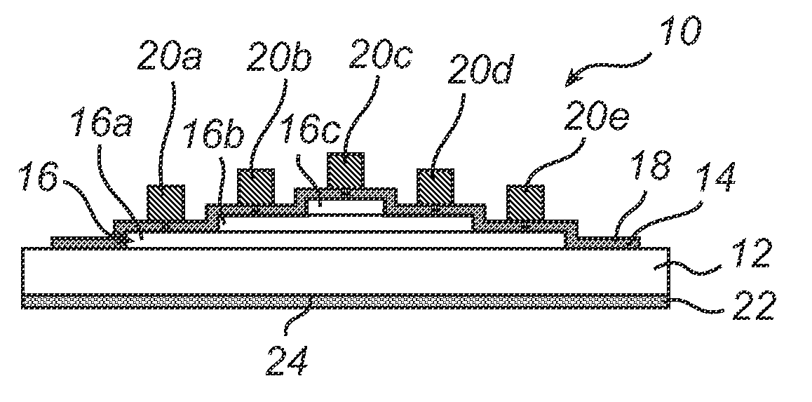
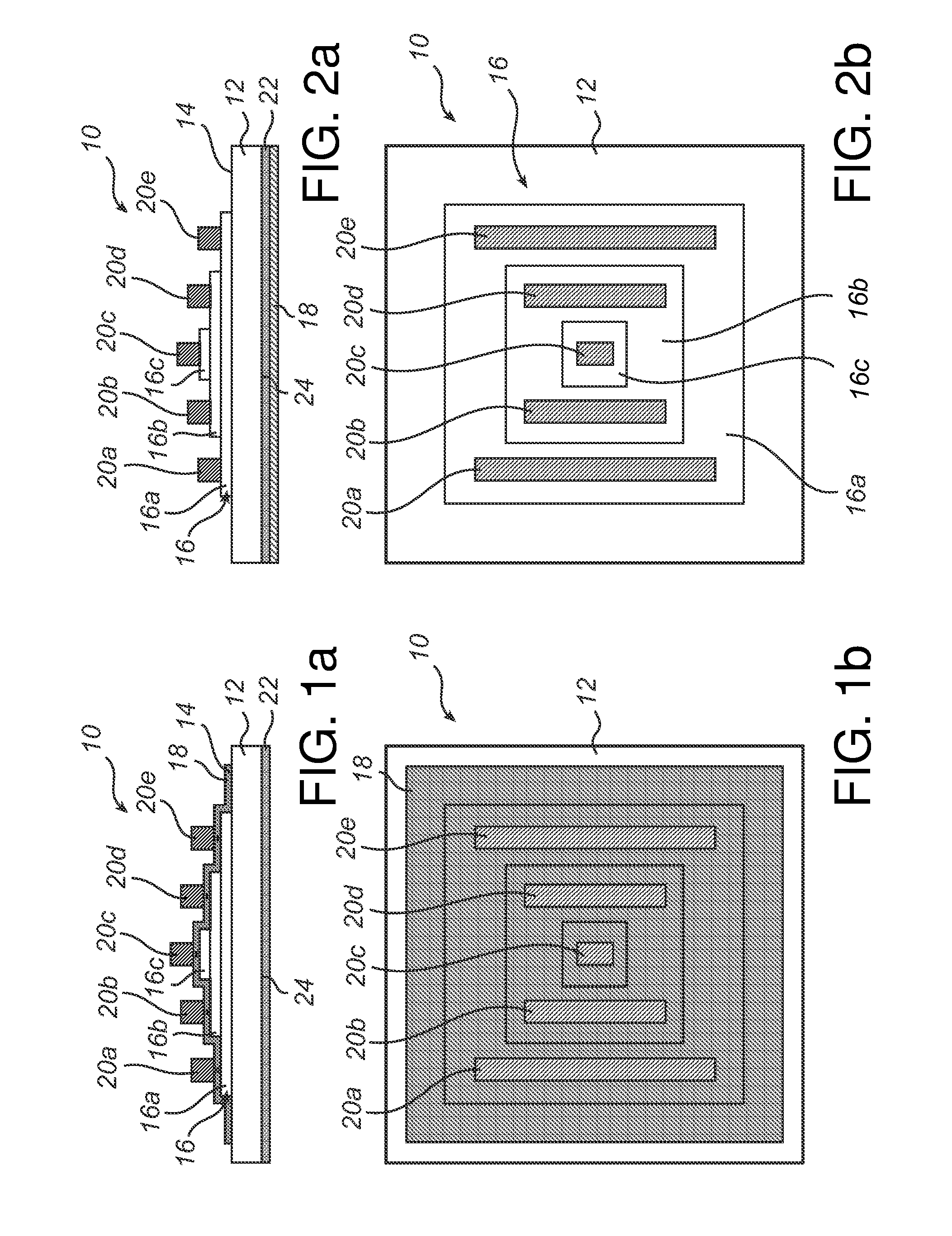
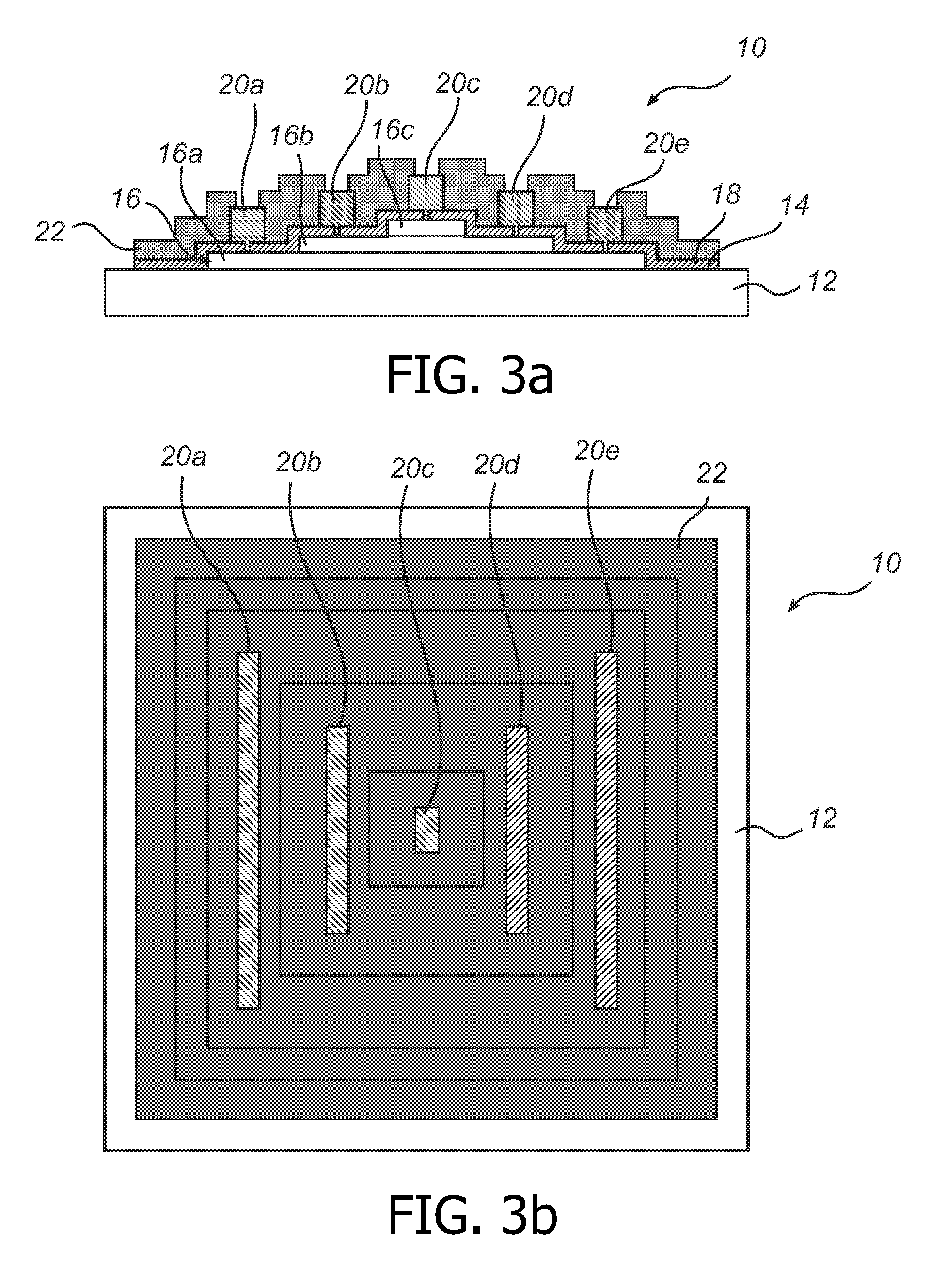
[0020]FIG. 1a is a cross-sectional side view and FIG. 1b is a top view of a semiconductor device 10 according to one embodiment of the invention.
[0021]The device 10 comprises a substrate 12, e.g. a silicon plate. On the front surface 14 of the substrate 12, a transistor 16 is processed. The transistor 16 comprises from bottom to top a collector 16a, a base 16b, and an emitter 16c in a mesa configuration. Further, a first dielectric passivation layer 18 is provided over the front surface 14 of the substrate 12, i.e. on the transistor 16 and on a portion of the front surface 14 of the sub...
PUM
 Abstract
Description
Claims
Application Information
 - R&D Engineer
- R&D Manager
- IP Professional
- Industry Leading Data Capabilities
- Powerful AI technology
- Patent DNA Extraction
Browse by: Latest US Patents, China's latest patents, Technical Efficacy Thesaurus, Application Domain, Technology Topic, Popular Technical Reports.
© 2024 PatSnap. All rights reserved.Legal|Privacy policy|Modern Slavery Act Transparency Statement|Sitemap|About US| Contact US: help@patsnap.com