Inductor structure

a technology of inductor and inductor coil, which is applied in the direction of inductance, basic electric elements, coils, etc., can solve the problems of reducing the space available to other transistors and the size of the chip, increasing the parasitic capacitance between the carrier and the coil, and prolonging the delay time of the electronic elements. , to achieve the effect of increasing the inductance, enhancing the mutual induction, and increasing the inductan

Inactive Publication Date: 2011-05-12
NATIONAL TSING HUA UNIVERSITY
View PDF6 Cites 6 Cited by
  • Summary
  • Abstract
  • Description
  • Claims
  • Application Information

AI Technical Summary

Benefits of technology

As mentioned above, the conventional technology increases the area of elements or vertically stacks the coils to increase the inductance. However, the present invention uses the characteristic of the electromagnetism of the ma

Problems solved by technology

However, a greater winding area in the chip not only reduces the space available to other transistors and the size of the chip but also increases the parasitic capacitance between the carrier and the coil.
The higher parasitic capacitance prolongs the delay time of the electronic elements, and decreases the energy

Method used


Image

  • Inductor structure
  • Inductor structure
  • Inductor structure

Examples


Embodiment Construction

Below, the technical contents of the present invention will be described in detail in cooperation with the drawings.

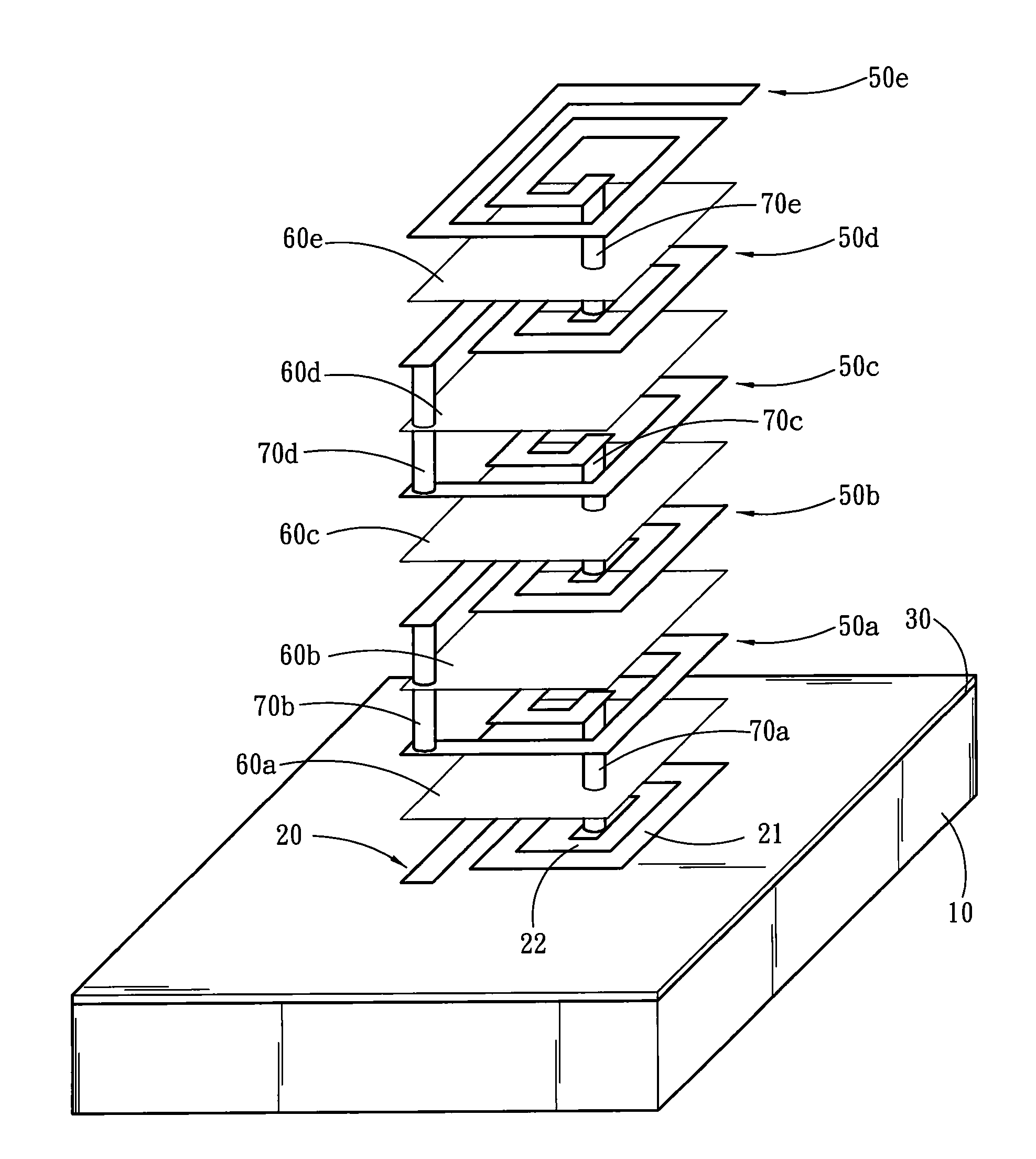
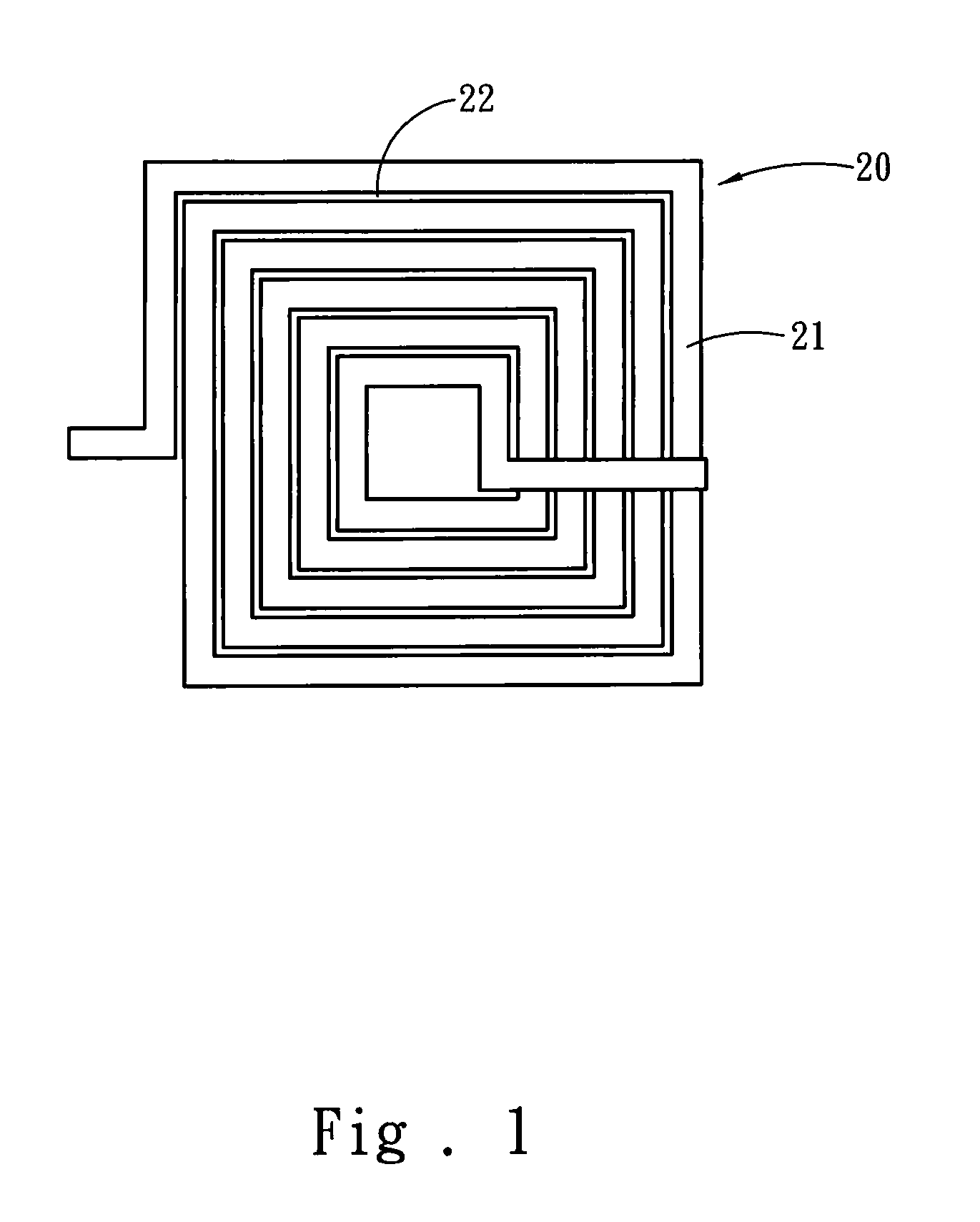
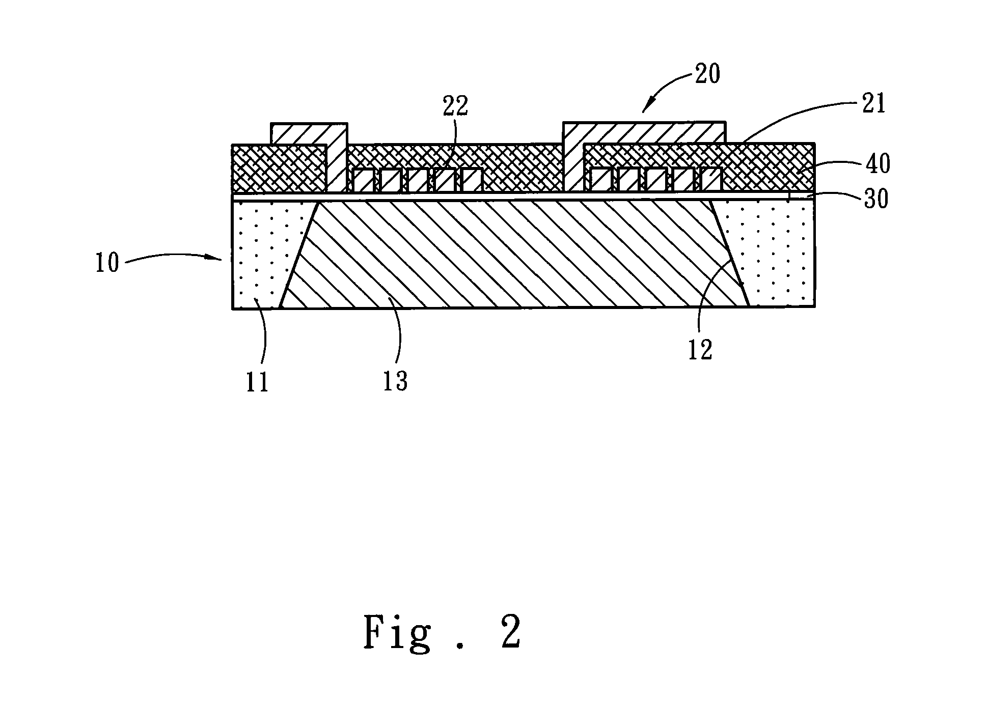
Refer to FIG. 1 and FIG. 2 respectively a schematic diagram of a conductive patterned film and a sectional view of an improved inductor structure according to a preferred embodiment of the present invention. The present invention proposes an improved inductor structure, which applies to the semiconductor field, particularly to a system-on-chip, and which comprises a substrate 10, a first conductive patterned film 20, a first insulating layer 30 formed between the substrate 10 and the first conductive patterned film 20, and a protective layer 40 covering on the surface of the first conductive patterned film 20. The substrate 10 has a base 11 and an accommodation portion 12 formed in the base 11. A magnetic material is filled into the accommodation portion 12 to form a magnetic region 13. The base 11 is made of a material selected from a group consisting of silicon, alum...


PUM


Abstract

The present invention discloses an improved inductor structure, which applies to the semiconductor field, particularly to a system-on-chip, and which comprises a substrate, a first conductive patterned film, and a first insulating layer formed between the substrate and the first conductive patterned film. The substrate has a base and an accommodation portion formed in the base. A magnetic material is filled into the accommodation portion to form a magnetic region. The accommodation portion is fabricated via etching the base or drilling a through-hole in the base. A plurality of conductive wires is arranged in a spiral way to form the first conductive patterned film. A protective layer covers the surface of the first conductive patterned film and isolates the contact of the first conductive patterned film and moisture.

Description

FIELD OF THE INVENTIONThe present invention relates to an improved inductor structure, particularly to an improved inductor structure installed on a special substrate and applied to the semiconductor field.BACKGROUND OF THE INVENTIONWith the progress of the semiconductor technology, most of circuit systems now can be fabricated into a single chip, i.e. the so-called system-on-chip or SOC for short. A system-on-chip usually has oscillation circuits and thus needs capacitors and inductors. For a capacitor or an inductor, the stored energy is proportional to the area of the element. Thus, an inductor having higher inductance needs a greater area. An U.S. Pat. No. 6,600,403 disclosed a planar inductor, wherein a coil is helically formed on a carrier to function as an induction loop. This prior art uses the spiral structure to increase the cross-section area of the equivalent conductor. For achieving a higher inductance, it is necessary to increase the coil length and the winding area. H...

Claims


Application Information

Patent Timeline
IPC IPC(8): H01F5/00
CPCH01F17/045H01F17/0013
Inventor DUH, JENQ-GONGLAI, YUAN-TAI
Owner NATIONAL TSING HUA UNIVERSITY
Why Eureka
Try Eureka