Hybrid integrated optical module

a technology of integrated optical modules and integrated modules, applied in the direction of optical elements, waveguide devices, instruments, etc., to achieve the effect of suppressing connection loss and high coupling efficiency

Inactive Publication Date: 2011-05-12
FURUKAWA ELECTRIC CO LTD
View PDF7 Cites 9 Cited by
  • Summary
  • Abstract
  • Description
  • Claims
  • Application Information

AI Technical Summary

Benefits of technology

[0010]The present invention aims at providing a hybrid integrated optical module ha

Problems solved by technology

Further, when, for optically coupling the respective waveguides of a semiconductor device and a silica-based PLC device, the gap between the waveguides is adjusted from a zero point where both devices contact each other at the respe

Method used


Image

  • Hybrid integrated optical module
  • Hybrid integrated optical module
  • Hybrid integrated optical module

Examples


first embodiment

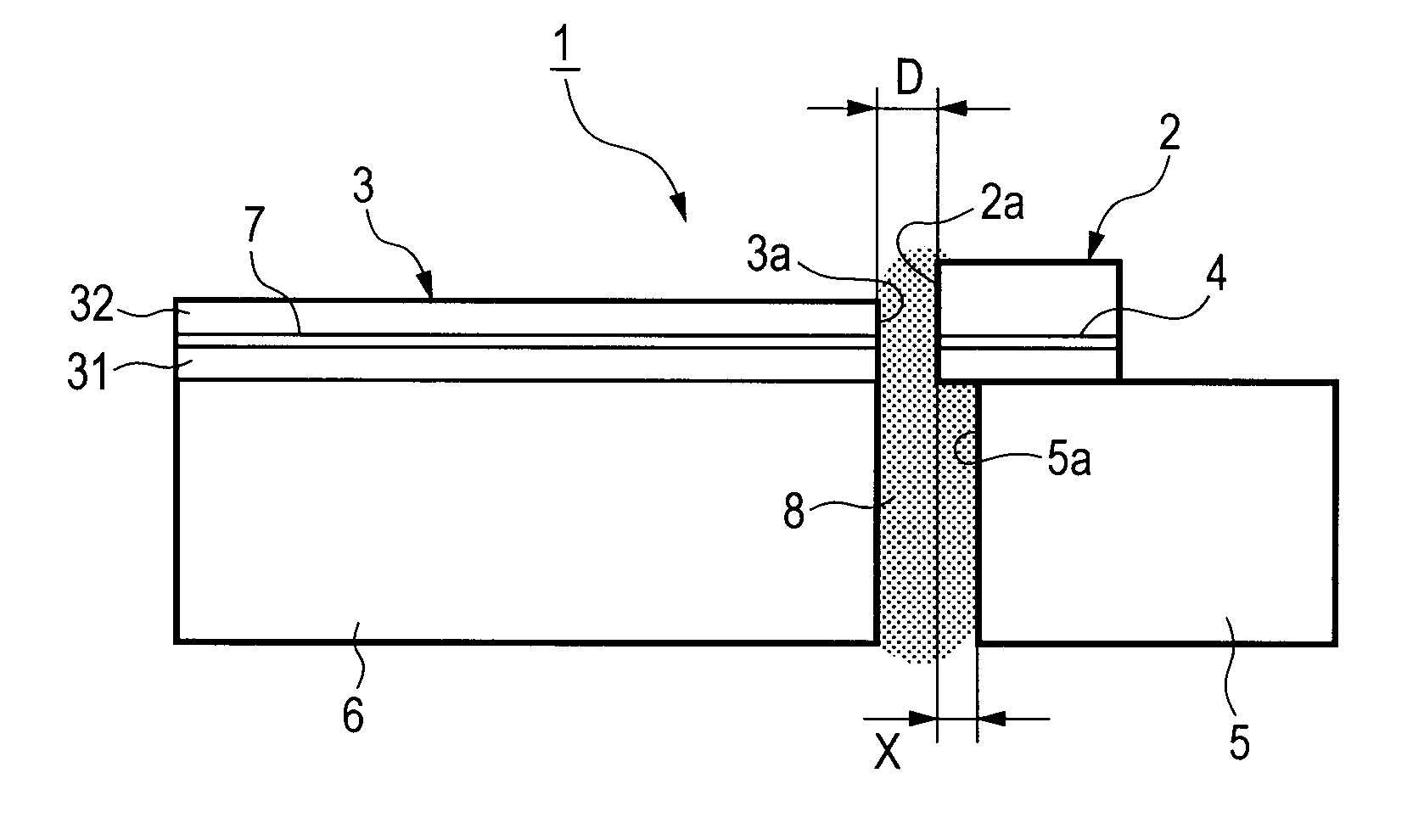
[0025]First, a hybrid integrated optical module 1 according to a first embodiment of the present invention will be explained according to FIG. 1 and FIG. 2. FIG. 1 is a conceptual diagram showing a basic configuration of the hybrid integrated optical module 1 and a cross-section thereof.

[0026]The hybrid integrated optical module 1 is an optical module integrating a semiconductor waveguide device 2 as a first waveguide device and a planar lightwave circuit chip 3 as a second waveguide device.

[0027]The semiconductor waveguide device (hereinafter, called “semiconductor chip”) 2 has a semiconductor waveguide 4 and is mounted on a silicon (Si) bench 5 as a first substrate.

[0028]The planar lightwave circuit chip (hereinafter, called “PLC chip”) 3 is provided with a PLC substrate 6 as a second substrate and an optical waveguide 7 formed on the PLC substrate 6. The PLC substrate 6 is a substrate made of silicon, silica, or the like. The PLC chip 3 has an optical waveguide 7 formed on the PL...

second embodiment

[0051]Next, a hybrid integrated optical module 1A according to a second embodiment of the present invention will be explained with reference to FIG. 5 and FIG. 6. FIG. 5 is a conceptual diagram showing a basic configuration of the hybrid integrated optical module 1A and a cross section thereof.

[0052]The hybrid integrated optical module 1A is an optical module integrating a semiconductor chip 2A as a first waveguide device and two PLC chips 3A and 3B as second waveguide devices.

[0053]The semiconductor chip 2A has a semiconductor waveguide 4A which can transmit light from an input side to an output side and is mounted on a Si bench 5A. The semiconductor waveguide 4A extends from one end face 2b of the semiconductor chip 2A to the other end face 2c thereof.

[0054]The PLC chip 3A includes a PLC substrate 6A as a second substrate and an optical waveguide 7A formed on the PLC substrate 6A. Further, the PLC chip 3B includes a PLC substrate 6B as a second substrate and an optical waveguide 7...

third embodiment

[0065]Next, a hybrid integrated optical module 1B according to a third embodiment of the present invention will be explained with reference to FIG. 7 to FIG. 9.

[0066]FIG. 7 is a plan view showing a basic configuration of the hybrid integrated optical module 1B. FIG. 8 is a cross-sectional view taken along the line A-A of FIG. 7 and shows a cross-sectional structure of a PLC chip 3C. Further, FIG. 9 is a cross-sectional view taken along the line B-B of FIG. 7 and shows a cross-sectional structure of a semiconductor waveguide part of a semiconductor chip 2B.

[0067]The hybrid integrated optical module 1B is an optical module integrating a semiconductor chip 2B as a first waveguide device which is fixed on a silicon substrate 5B as a first substrate and a PLC chip 3C as a second waveguide device as shown in FIG. 7.

[0068]The PLC chip 3C includes a PLC substrate 6C and two linear optical waveguides 15 and 16 formed on the PLC substrate 6C as shown in FIG. 7 and FIG. 8. Each of the optical ...


PUM

PropertyMeasurementUnit
Efficiencyaaaaaaaaaa
Distanceaaaaaaaaaa

Abstract

The present invention provides a hybrid integrated optical module having a high coupling efficiency by suppressing a connection loss between waveguides. A hybrid integrated optical module according to an embodiment of the present invention is an optical module which integrates a semiconductor chip and a PLC chip. The semiconductor chip has a semiconductor waveguide and is mounted on a Si bench. The PLC chip includes a PLC substrate and an optical waveguide formed on the PLC substrate. An end face of the semiconductor chip protrudes from an end face of the Si bench toward the PLC chip side by a protrusion amount X. Gap adjustment (adjustment of a distance D) between the semiconductor waveguide and the optical waveguide becomes possible by setting a position where the end face of the semiconductor chip is brought into contact with an end face of the PLC chip to be a reference position (zero point).

Description

BACKGROUND OF THE INVENTION[0001]1. Field of the Invention[0002]The present invention relates to a hybrid integrated optical module which integrates a first waveguide device having a semiconductor waveguide and is mounted on a first substrate, and a second waveguide device.[0003]2. Description of the Related Art[0004]Along with the spread and the progress of an optical communication network, an optical component to be used in an optical communication system has been progressing to have a high functionality. The optical component includes an active optical component to emit or receive signal light, a passive optical component to branch / combine or to de-multiplex / multiplex the signal light, an optical fiber used for a signal light transmission line, and the like, and the need of a high functionality and a low cost is increased for each of the optical components. Among them, the main active optical components is a semiconductor material based device such as a semiconductor laser elemen...

Claims


Application Information

Patent Timeline
IPC IPC(8): G02B6/12H01P11/00
CPCY10T29/49016G02B6/4225
Inventor AKUTSU, TAKESHIHASEGAWA, JUNICHINARA, KAZUTAKA
Owner FURUKAWA ELECTRIC CO LTD
Why Eureka
Try Eureka